


Forbes: Applied Materials Going Solar - 500 Beiträge pro Seite
eröffnet am 30.08.06 18:04:07 von
neuester Beitrag 01.07.19 12:13:16 von
neuester Beitrag 01.07.19 12:13:16 von
Beiträge: 230
ID: 1.079.811
ID: 1.079.811
Aufrufe heute: 0
Gesamt: 43.688
Gesamt: 43.688
Aktive User: 0
ISIN: US0382221051 · WKN: 865177 · Symbol: AMAT
203,38
USD
+2,98 %
+5,88 USD
Letzter Kurs 02:00:00 Nasdaq
Neuigkeiten
| Applied Materials Aktien ab 5,80 Euro handeln - Ohne versteckte Kosten!Anzeige |
18.04.24 · dpa-AFX |
18.04.24 · dpa-AFX |
18.04.24 · dpa-AFX |
18.04.24 · dpa-AFX |
Werte aus der Branche Halbleiter
| Wertpapier | Kurs | Perf. % |
|---|---|---|
| 3,5000 | +33,59 | |
| 5.010,00 | +25,09 | |
| 4,0800 | +23,45 | |
| 3,0500 | +21,03 | |
| 9,0000 | +20,00 |
| Wertpapier | Kurs | Perf. % |
|---|---|---|
| 16,780 | -12,01 | |
| 7,4000 | -12,94 | |
| 5,2900 | -14,26 | |
| 4,4500 | -17,13 | |
| 13,590 | -22,56 |
Market Scan
Applied Materials Going Solar
R.M. Schneiderman, 08.28.06, 11:27 AM ET
Semiconductor production equipment maker Applied Materials' year-long effort to develop solar power technology could potentially be a major boon for the company's growth, according to a Monday report by Banc of America Securities.
"Over the past year Applied Materials has quietly begun a serious development effort in solar power technology," said Mark FitzGerald an analyst for the research firm.
"Solar is potentially as large...an opportunity for Applied Materials as their semiconductor business."
In July, Applied Matierals (nasdaq: AMAT - news - people ) acquired Applied Films, which supplies equipment used in making solar technology and energy-efficient glass. The deal was worth $464 million.
In order to make solar power a viable business, Applied Materials needs to find a way to make it more competitive with other fossil fuel alternatives, the analyst said.
"The opportunity requires that Applied Materials change the current economics of the solar power industry," said FitzGerald.
"The primary objective in solar power is to balance the goal of the most efficient solution…with the lowest cost. The problem with the current…technologies is that conversion efficiency is low and costs remain stubbornly high because of the high percentage of materials."
The analyst said solar power will likely be a three to five year research and development project for the company, as coal and natural gas continue to account for the bulk of U.S. electricity generation.
He maintained a price target of $16 and a "neutral" rating on the stock
Quelle: http://www.forbes.com/markets/2006/08/28/applied-materials-0…


Erstaunlicherweise gibt es keinen aktuellen Thread zu Applied Materials. Nach der Übernahme von Applied Films und damit den Einstieg in den boomenden Solarbereich sollte man die Aktie zumindest auf seine Watchlist nehmen und hier im Forum über die entwicklung diskutieren.
Zu Beginn hier die letzten News:
http://www.finanznachrichten.de/nachrichten-aktien/applied-m…
Datum Aktuelle Nachrichten: Sprache: Medien
30.08. / 09:07 Taiwan's TSMC buys machinery worth 533.63 mln twd from ... AFX News (GB)
29.08. / 19:07 APPLIED Materials - Aufwärtstendenz intakt GodmodeTrader (DE)
28.08. / 17:42 Applied Materials Going Solar Forbes (US)
24.08. / 21:31 Blocktrade bei Applied Materials, JP Morgan und The Gap GodmodeTrader (DE)
24.08. / 17:31 Applied Materials Inc.: neutral (JP Morgan) finanzen.net-Analysen (DE)
24.08. / 17:11 Applied Materials - Neues Rating BörseGo (DE)
23.08. / 21:19 Blocktrade bei Applied Materials, Intel und Yahoo GodmodeTrader (DE)
17.08. / 18:07 APPLIED Materials - Ab 16,04 $ geht es ab GodmodeTrader (DE)
17.08. / 16:49 Next Inning Technology Publishes Updated Outlooks for QuickLogic, ... PR Newswire (US)
17.08. / 10:31 Applied Materials Inc.: overweight (Prudential Financial) finanzen.net-Analysen (DE)
Datum Aktuelle Nachrichten: Sprache: Medien
17.08. / 08:55 Applied Materials Inc.: outperform (Thomas Weisel Partners) finanzen.net-Analysen (DE)
17.08. / 08:55 Applied Materials Inc.: neutral (UBS) finanzen.net-Analysen (DE)
16.08. / 19:27 SILICON STOCKS: Techs Edge Higher; Applied Materials Dips ... Morningstar (US)
16.08. / 18:47 Applied Materials - Neues Kursziel BörseGo (DE)
16.08. / 18:07 Applied Materials Inc.: neutral (Banc of America Sec.) finanzen.net-Analysen (DE)
16.08. / 18:07 Applied Materials Inc.: sector outperform (CIBC World Markets) finanzen.net-Analysen (DE)
16.08. / 17:47 Applied Materials skeptisch trotz Gewinnanstieg Reuters Deutschland (DE)
16.08. / 16:50 US-Technologieaktien: Applied Materials knickt ein de.internet.com (DE)
16.08. / 16:38 Applied Materials legt unterm Strich um 39 Prozent zu Computerwoche (DE)
06.07.2006, 15:34 Uhr
Applied Films erhält Großauftrag über Produktionsanlagen für mikromorphe Solarzellen
Alzenau - Applied Films, Anbieter von Dünnschicht-Produktionsanlagen, hat einen Großauftrag über Produktionssysteme für mikromorphe Dünnschichtsolarzellen erhalten. Auftraggeber ist Brilliant 234, ein 100%iges Tochterunternehmen von Q-Cells. Im Rahmen des Vertrages wurden drei integrierte Vakuumbeschichtungssysteme zur Produktion mikromorpher Solarzellen bestellt. Mit den Systemen werden die TCO-Frontkontaktschicht, das lichtabsorbierende Schichtsystem (a-Si/µc-Si) und der Rückseitenkontakt aufgebracht.
Nach Einschätzung von Applied Films stellt die mikromorphe Technologie bei Dünnschichtzellen die überlegene Technologie dar. Mit dieser Technologie hergestellte Zellen weisen aufgrund ihrer verbesserten spektralen Empfindlichkeit einen höheren Wirkungsgrad gegenüber amorphen Solarzellen auf, so das Unternehmen.
„Mit Applied Films haben wir einen Schlüssel-Anlagenlieferanten gefunden, der eindeutig zu den Technologie- und Innovationsführern in der Solarzellenherstellung zählt,“ so Anton Milner, CEO von Q-Cells. „Die kontinuierliche Weiterentwicklung unserer Technologie und Produktionsprozesse sind die Grundpfeiler unseres Erfolges. Dabei geht es sowohl um unsere Kerntechnologie für Siliziumwafer-basierte Hochleistungs-Solarzellen als auch die Kommerzialisierung von Dünnschicht-Technologien. Die große Expertise von Applied Films in Vakuumbeschichtungsprozessen für großflächige Substrate wird ein entscheidender Faktor für uns sein, unsere ehrgeizigen Ziele in den nächsten Jahren zu erreichen“, so Milner weiter.
Weitere Infos und News zum Thema Solarenergie
SolarWorld AG: Firmenprofil, Produkte, Presse-News, Kontakt
Q-Cells baut Produktion weiter aus - Ausblick für 2006 angehoben
RENIXX – Zum aktuellen Börsenkurs der Q-Cells AG
EEG-Vergütungsrechner für Strom aus Photovoltaik
Quelle: iwr/06.07.06/
http://www.iwr.de/news.php?id=8939
07.07.2006 22:26
Applied Materials Completes Acquisition of Applied Films
Applied Materials, Inc. announced today that it has completed the acquisition of Applied Films Corporation, a leading supplier of thin film deposition equipment used in manufacturing flat panel displays, solar cells, flexible electronics and energy-efficient glass.
"This is an important acquisition for Applied Materials (Nachrichten/Aktienkurs) that complements and extends our thin film nanomanufacturing technology capabilities and provides a number of exciting opportunities to expand our business into growing new markets," said Mike Splinter, president and CEO of Applied Materials.
Applied Films' operations are now part of Applied Materials' New Business and New Products Group, which is managed by Mark Pinto, senior vice president and chief technology officer.
Under the terms of the agreement signed on May 4, 2006, Applied Materials will pay $28.50 per share in cash for each outstanding share of Applied Films common stock, which represents a total purchase price of approximately $464 million, or approximately $300 million net of Applied Films' existing cash and marketable securities. As part of the acquisition, Applied Materials assumed Applied Films' stock options and other equity awards outstanding immediately prior to the closing of the transaction.
This press release contains forward-looking statements relating to Applied Materials' acquisition of Applied Films and expected benefits of the transaction, including growth opportunities in existing and emerging markets, technology leadership and improved product capabilities. These statements are subject to known and unknown risks and uncertainties that could cause actual results to differ materially from those stated or implied, including but not limited to: the successful integration and performance of the acquired business; sustainability of demand in the nanomanufacturing technology industry, and broadening of demand for emerging applications such as solar cells and flexible electronics, which are subject to many factors, including global economic conditions, business spending, consumer confidence, demand for electronic products and integrated circuits, and geopolitical uncertainties; Applied Materials' ability to develop, deliver and support a broad range of products and to expand its markets and develop new markets; the ability to obtain and protect intellectual property rights in key technologies; the retention of key employees; the ability to realize synergies expected to result from the acquisition; successful commercialization of purchased technologies; the effectiveness of internal controls; unknown, underestimated or undisclosed commitments or liabilities; and other risks described in Applied Materials' Forms 10-K, 10-Q and 8-K filed with the Securities and Exchange Commission. All forward-looking statements are based on management's estimates, projections and assumptions as of the date hereof and Applied Materials assumes no obligation to update any such statement.
Applied Materials, Inc. (Nasdaq:AMAT) is the global leader in nanomanufacturing technology(TM) solutions for the electronics industry with a broad portfolio of innovative equipment, service and software products. At Applied Materials, we apply nanomanufacturing technology to improve the way people live. Learn more at www.appliedmaterials.com.
Quelle: Business Wire
Thema: Applied Materials meldet Gewinnanstieg um 39 Prozent, übertrifft Erwartungen [Thread-Nr: 1077127]
http://www.wallstreet-online.de/community/thread/1077127-1.h…
http://www.wallstreet-online.de/community/thread/1077127-1.h…
Trading Spotlight
Glück gehabt, wollte bis morgen einen Thread zu AMAT einstellen
Hoch interessant wird der 5. September, wenn AMAT bei ihrem Webcast die zukünftigen Solaraktivitäten vorstellt.
Quartalserlös + 56%, Quartalsgewinn + 38%
Nebenbei Cash in Höhe von 2,83 Milliarden USD
AMAT gehört seit ca. 2 Monaten zum Portfolio von Wealthdaily, dem Börsenbrief von Jeff Siegel, dessen Empfehlungen in den letzten Jahren immer sehr fundiert und erfolgreich waren, siehe Evergreen Solar, Pacific Ethanol uvm.
Wir werden noch viel Freude an dieser Aktie haben

Antwort auf Beitrag Nr.: 23.695.541 von Isti08 am 31.08.06 09:57:58Hallo Ist08,
Du bringst ja eine richtig gute Stimmung hier rein in den neuen Thread. Egal wer ihn eröffnet hat, Dein Posting zeigt deutlich, daß Du stärker involviert bist. Schlage vor, daß Du die Initiative übernimmst.
Im übrigen hat mich gewundert, daß die Leute hier über Gott und die Welt posten und sich wahnsinnig bei Pennystocks und Nebenwerten engagieren, eine Aktie wie Applied Films/Applied Materials aber mehr oder weniger ignorieren. Aber auch in den USA
war Amat in letzter Zeit nicht gerade ein Renner.
Bin gespannt auf den 5. September.
Gruss
N.
Das ist die Ruhe vor dem Sturm in den USA.
Vor Überraschungen ist man bei AMAT nie sicher, so wurde vor 2 Tagen kurz vor Börsenschluss ein einziges Paket mit 1000k verkauft, um mit einem 1,5k Päckchen anschließend den Kurs auf TH zu ziehen
Natürlich wäre es dumm, AMAT als Kurzfristinvest zu sehen. Das Kursziel einiger Analysten und auch Siegel liegt bei 22 USD bis Jahresende und das wären immerhin 30%, zusätzlich wird Dividende gezahlt und man ist in einen Konzern investiert, dessen Cashbestand Hoffnung auf strategische Übernahmen macht, deren Ausmaß man noch gar nicht abschätzen kann
Der Kurs ist zu hoch für die meisten Pusherblättchen, deshalb ist die Aktie hier auch völlig unbekannt.
Vor Überraschungen ist man bei AMAT nie sicher, so wurde vor 2 Tagen kurz vor Börsenschluss ein einziges Paket mit 1000k verkauft, um mit einem 1,5k Päckchen anschließend den Kurs auf TH zu ziehen

Natürlich wäre es dumm, AMAT als Kurzfristinvest zu sehen. Das Kursziel einiger Analysten und auch Siegel liegt bei 22 USD bis Jahresende und das wären immerhin 30%, zusätzlich wird Dividende gezahlt und man ist in einen Konzern investiert, dessen Cashbestand Hoffnung auf strategische Übernahmen macht, deren Ausmaß man noch gar nicht abschätzen kann
Der Kurs ist zu hoch für die meisten Pusherblättchen, deshalb ist die Aktie hier auch völlig unbekannt.
bin schon seit 3 Wochen drin und rechne mit Durchbruch der $ 17,00 mit einem Ausbruch! Hier noch heutige schöne Infos:
APPLIED MATERIALS INC /DE
--------------------------------------------------------------------------------
31-Aug-2006
Quarterly Report
Item 2. Management's Discussion and Analysis of Financial Condition and Results of Operations
Certain information contained in this Quarterly Report on Form 10-Q is forward-looking in nature. All statements in this Quarterly Report on Form 10-Q, including those made by management of Applied Materials, Inc. and its subsidiaries (Applied or the Company), other than statements of historical fact, are forward-looking statements. Examples of forward-looking statements include statements regarding Applied's future financial results, operating results, business strategies, cash generation, cash deployment strategies, projected costs, products, competitive positions, management's plans and objectives for future operations, acquisitions and joint ventures, growth opportunities, and legal proceedings, as well as industry trends. These forward-looking statements are based on management's estimates, projections and assumptions as of the date hereof and include the assumptions that underlie such statements. Forward-looking statements may contain words such as "may," "will," "should," "could," "would," "expect," "plan," "anticipate," "believe," "estimate," "predict," "potential," and "continue," the negative of these terms, or other comparable terminology. Any expectations based on these forward-looking statements are subject to risks and uncertainties and other important factors, including those discussed below and in Part II, Item 1A, Risk Factors. Other risks and uncertainties are disclosed in Applied's prior Securities and Exchange Commission (SEC) filings, including its Annual Report on Form 10-K for the fiscal year ended October 30, 2005. These and many other factors could affect Applied's future financial operating results and could cause actual results to differ materially from expectations based on forward-looking statements made in this report or elsewhere by Applied or on its behalf. Applied undertakes no obligation to revise or update any forward-looking statements.
Overview
Applied develops, manufactures, markets and services integrated circuit fabrication equipment, providing nanomanufacturing technologytm solutions for the global semiconductor and semiconductor-related industry. Product development and manufacturing activities occur primarily in North America, Europe and Israel. Applied's broad range of equipment, service and related products are highly technical and, as a result, are sold through a direct sales force. Customer demand for spare parts and services is fulfilled through a global spare parts distribution system and by trained service engineers located in close proximity to customer sites around the world.
As a supplier to the global semiconductor and semiconductor-related industry, Applied's results are driven primarily by worldwide demand for integrated circuits, which in turn depends on end-user demand for electronic products. The global semiconductor and semiconductor-related industry is volatile, and consequently Applied's operating results have reflected this volatility.
The following table presents certain significant measurements for the three and nine months ended July 31, 2005 and July 30, 2006:
Nine Months
Three Months Ended Ended
July 31, July 30, July 31, July 30,
2005 2006 % Change 2005 2006 % Change
(In millions, except per share amounts and percentages) (In millions, except per share amounts and percentages)
New orders $ 1,468 $ 2,670 82 % $ 4,696 $ 7,199 53 %
Net sales $ 1,632 $ 2,543 56 % $ 5,274 $ 6,649 26 %
Gross margin $ 717 $ 1,223 71 % $ 2,326 $ 3,106 34 %
Gross margin percent 43.9 % 48.1 % 10 % 44.1 % 46.7 % 6 %
Net income $ 370 $ 512 39 % $ 963 $ 1,068 11 %
Earnings per diluted share $ 0.23 $ 0.33 46 % $ 0.58 $ 0.67 16 %
Operating results for fiscal 2005 reflected decreased global customer fab utilization and reduced or delayed capacity additions as a result of excess inventories and slowing demand for integrated circuits. During this period, Applied focused on lowering costs, improving efficiencies, reducing cycle time, and bringing new products to market. Applied also generated strong cash flow and returned value to stockholders by repurchasing stock and paying cash dividends. During the fourth quarter of fiscal 2005, customer demand began to increase.
--------------------------------------------------------------------------------
Table of Contents
Customer demand further improved in the first nine months of fiscal 2006, resulting in higher orders and revenues. During this period, Applied's customers increased both high-volume production and leading-edge 65 nanometer (nm) and 45nm chip development. Results for this period also reflected Applied's continued focus on cost controls. Operating performance was offset during the nine months in part by restructuring and asset impairment charges associated with the real estate and facilities disinvestment that commenced during the first fiscal quarter, by equity-based compensation expenses and by an in-process research and development expense (see Notes 1, 8 and 12 of the Notes to Consolidated Condensed Financial Statements).
During the third quarter of fiscal 2006, Applied completed certain transactions in support of the Company's long-term growth strategy. Management believes that these transactions will enhance Applied's ability to extend its nanomanufacturing capabilities into adjacent and new markets, including: color filters for flat panel displays, solar energy, flexible electronics, energy-efficient glass and track solutions for semiconductor manufacturing. These transactions included the acquisition of Applied Films Corporation (Applied Films), and the formation of a joint venture with Dainippon Screen Mfg. Co., Ltd. (Screen) (see Note 12 of the Notes to Consolidated Condensed Financial Statements). The results of operations of these companies subsequent to the acquisition dates were not material for the third quarter of fiscal 2006. During the fourth quarter of fiscal 2006, Applied purchased certain parts cleaning and recycling assets in Singapore from UMS Solutions Pte. Ltd. (UMS Solutions) a wholly-owned subsidiary of Norelco UMS Holdings Limited (see Note 15 of the Notes to Consolidated Condensed Financial Statements).
Applied's long-term opportunities depend in part on the successful execution of its growth strategy, including increasing market share in existing markets, expanding into related markets, and cultivating new markets and business models. These opportunities are also subject to: (1) global economic conditions;
(2) advanced technology and/or capacity requirements of integrated circuit manufacturers and their capital investment trends; (3) the profitability of integrated circuit manufacturers; (4) supply and demand for integrated circuits;
(5) realization of the anticipated benefits of business combinations;
(6) continued investment in research, development and engineering (RD&E); and
(7) the relative competitiveness of Applied's equipment and service products. For these and other reasons set forth in Part II, Item 1A, Risk Factors, which are incorporated by this reference, Applied's prior consolidated results of operations are not necessarily indicative of future operating results.
Results of Operations
Applied received new orders of $2.7 billion for the third quarter of fiscal 2006, compared to $2.5 billion for the second quarter of fiscal 2006 and $1.5 billion for the third quarter of fiscal 2005. New orders for the third quarter of fiscal 2006 increased by 7 percent from the preceding quarter and increased by 82 percent from the third quarter of fiscal 2005. The increase in new orders from the previous quarter was broad-based for virtually all products, and was primarily attributable to increased customer demand from memory manufacturers and foundries. Orders increased in Japan, Taiwan, Southeast Asia and China, North America and Europe, and decreased in Korea.
New orders by region for the past two consecutive quarters were as follows:
Three Months Ended
April 30, July 30,
2006 2006
($) (%) ($) (%)
(In millions, except percentages)
Taiwan 479 19 566 21
Japan 434 17 534 20
North America(*) 444 18 475 18
Korea 542 22 435 16
Southeast Asia and China 350 14 418 16
Europe 239 10 242 9
Total 2,488 100 2,670 100
(*) Primarily the United States.
--------------------------------------------------------------------------------
Table of Contents
Applied's backlog for the most recent three fiscal quarters was as follows:
$3.3 billion at July 30, 2006, $2.9 billion at April 30, 2006 and $2.7 billion at January 29, 2006. Backlog has been adjusted to reflect the acquisition of Applied Films. Backlog consists only of orders for which written authorizations have been accepted, shipment dates within 12 months have been assigned and revenue has not been recognized. Due to the potential for customer changes in delivery schedules or cancellation of orders, Applied's backlog at any particular time is not necessarily indicative of actual sales for any future periods.
Demand for integrated circuit manufacturing equipment has historically been volatile as a result of sudden changes in integrated circuit supply and demand and other factors, including rapid technological advances in the integrated circuit fabrication process. As a result of these conditions, there were fluctuations in Applied's net sales throughout fiscal year 2005. During fiscal 2005, net sales increased from $1.8 billion in the first fiscal quarter to $1.9 billion in the second fiscal quarter, decreased to $1.6 billion in the third fiscal quarter, and increased to $1.7 billion in the fourth fiscal quarter. Net sales during the first fiscal quarter of 2006 increased to $1.9 billion and then to $2.2 billion during the second fiscal quarter of 2006, and then to $2.5 billion during the third fiscal quarter of 2006 due to broad-based customer demand resulting from rising fab utilization and investments in advanced technology.
Net sales by region for the three and nine months ended July 31, 2005 and July 30, 2006 were as follows:
Three Months Ended Nine Months Ended
July 31, July 30, July 31, July 30,
2005 2006 2005 2006
($) (%) ($) (%) ($) (%) ($) (%)
(In millions, except percentages)
Taiwan 381 23 688 27 1,199 23 1,515 23
North America(*) 351 22 418 17 1,053 20 1,197 18
Japan 333 20 415 16 1,000 19 1,074 16
Korea 248 15 412 16 867 16 1,307 20
Southeast Asia and China 141 9 382 15 473 9 807 12
Europe 178 11 228 9 682 13 749 11
Total 1,632 100 2,543 100 5,274 100 6,649 100
(*) Primarily the United States.
Gross margin percentage was 48.1 percent for the third quarter of fiscal 2006, compared to 46.5 percent for the second quarter of fiscal 2006 and 43.9 percent for the third quarter of fiscal 2005. Gross margin during the three and nine months ended July 30, 2006 included $9 million and $27 million of equity-based compensation expense, respectively. The increase in the gross margin percentage for the third quarter of fiscal 2006 from that of the previous quarter and from the third quarter of fiscal 2005 was principally attributable to the combination of improved revenue levels, decreased product costs and increased manufacturing volume and absorption, partially offset by increased variable compensation.
Operating expenses include expenses related to RD&E, marketing and selling (M&S), general and administrative (G&A), and restructuring and asset impairments. Expenses related to RD&E, M&S and G&A were $545 million for the third quarter of fiscal 2006, compared to $485 million for the second quarter of fiscal 2006 and $414 million for the third quarter of fiscal 2005. Higher total operating expenses during the three and nine months ended July 30, 2006 as compared to the same periods in 2005, were principally attributable to increased variable compensation, equity-based compensation, and early spending on the Company's business transformation initiative, partially offset by savings resulting from Applied's continued focus on controlling its overall cost structure. Equity-based compensation expenses for the three and nine months ended July 30, 2006 totaled $45 million and $134 million, respectively. During the third quarter of fiscal 2006, Applied launched the planning stage of its multi-year business transformation initiative, which is expected to include the design of new company-wide business processes and the transition to a single-vendor software system to perform various functions, such as order management and manufacturing control.
--------------------------------------------------------------------------------
Table of Contents
During the third quarter of fiscal 2006, Applied recorded an in-process research and development (IPR&D) expense in the amount of $14 million related to the acquisition of Applied Films that was reported as RD&E in the Consolidated Condensed Statement of Operations. Applied's methodology for allocating the purchase price relating to purchase acquisitions to IPR&D was determined through established valuation techniques. The IPR&D was expensed upon acquisition because technological feasibility had not been established and no future alternative uses existed. No IPR&D expense was recorded during the nine months ended July 31, 2005 (see Note 12 of the Notes to Consolidated Condensed Financial Statements).
The results of operations from Applied Films and the Sokudo joint venture were not material for the third quarter of fiscal 2006 and have not been included in the Condensed Consolidated Statement of Operations; these results will be included in Applied's fourth quarter of fiscal 2006.
On January 24, 2006, Applied's Board of Directors approved a plan to disinvest a portion of Applied's real estate and facilities portfolio (the Plan). Under the Plan, during the first quarter of fiscal 2006, properties with an estimated fair value of $56 million were reported as assets held-for-sale and reclassified from property, plant and equipment on the Consolidated Condensed Balance Sheet. Applied recorded a pre-tax asset impairment charge of $124 million during the first quarter of fiscal 2006 to write down the following properties to fair value: facilities in Narita, Japan; Chunan, Korea; Danvers, Massachusetts; and 26 acres of unimproved land in Hillsboro, Oregon. During the first quarter of fiscal 2006, Applied also recorded a pre-tax charge in the amount of $91 million for future lease obligations that were scheduled to continue through fiscal 2014 related to the closure of its Hayward, California facility as part of the Plan. During the third quarter of fiscal 2006, Applied sold the Danvers, Massachusetts facility for net proceeds of $16 million and recognized a gain of $4 million. Applied is actively marketing the remaining properties, and management believes that they will be sold within 12 months of the date that they were classified as held-for-sale.
During the third quarter of fiscal 2006, Applied recognized a net benefit of $3 million, consisting of a $4 million gain on the Danvers sale, partially offset by $1 million in costs associated with the facilities disinvestment under the Plan initiated in the first quarter of fiscal 2006. During the second quarter of fiscal 2006, Applied recognized a net benefit of $2 million, consisting of $4 million in adjustments associated with fiscal 2003 and 2004 restructuring actions, partially offset by $2 million in costs associated with the Plan.
Net interest income was $42 million and $37 million for the three months ended July 30, 2006 and July 31, 2005, respectively, and $121 million and $95 million for the nine months ended July 30, 2006 and July 31, 2005, respectively. Higher net interest income during the nine months ended July 30, 2006 was primarily due to higher average portfolio yields, as well as a decrease in interest expense as a result of the repayment of scheduled debt maturities in September 2005.
The income tax rate for the third quarter of fiscal 2006 was 29.1 percent, compared to 31.3 percent for the second quarter of fiscal 2006 and 22.4 percent for the first quarter of fiscal 2006. The income tax rate for the third quarter of fiscal 2006 included benefits of $34 million due primarily to a favorable resolution of audits of prior years' income tax filings. The first quarter tax rate includes the tax impact of the restructuring and asset impairment charges related to the real estate and facilities disinvestment plan (see Note 8 of Notes to Consolidated Condensed Financial Statements). The income tax rate for the third quarter of fiscal 2005 was a benefit of 8.9 percent, which included benefits of $118 million due to a favorable resolution of audits of prior years' income tax filings and $14 million relating to a change in estimate with respect to export tax benefits. The effective income tax rate is highly dependent on the geographic composition of worldwide earnings, tax regulations for each region, non-tax deductible expenses incurred in connection with acquisitions and the availability of tax credits. Management carefully monitors these factors and timely adjusts the effective income tax rate accordingly.
--------------------------------------------------------------------------------
Table of Contents
Financial Condition, Liquidity and Capital Resources
During the nine months ended July 30, 2006, cash, cash equivalents and
investments decreased by $828 million from $6.0 billion as of October 30, 2005
to $5.2 billion as of July 30, 2006.
Cash, cash-equivalents and investments consisted of the following:
October 30, July 30,
2005 2006
(In millions)
Cash and cash equivalents $ 990 $ 1,308
Short-term investments 2,343 1,524
Long-term investments 2,652 2,325
Total cash, cash-equivalents and investments $ 5,985 $ 5,157
During the second quarter of fiscal 2006, Applied changed its accounting method for certain fixed-income investments, which resulted in the reclassification of these investments from current assets to long-term investments. As a result, prior period balances have been reclassified to conform to the current period's presentation. This accounting method is based on the contractual maturity dates of fixed-income securities as current or long-term, while the prior classification was based on the nature of the securities and the availability for use in current operations. Applied believes this method is preferable as it is more reflective of Applied's assessment of the timing of when such securities are expected to be converted to cash. Accordingly, certain fixed-income investments of $2.6 billion have been reclassified from short-term investments to long-term investments in the October 30, 2005 Consolidated Condensed Balance Sheet to conform to the fiscal 2006 financial statement presentation. In connection with this reclassification, short-term deferred taxes have been reclassified to long-term deferred taxes. There have been no changes in Applied's investment policies or practices associated with this change in accounting method.
In addition, $50 million of long-term equity securities previously reported in other long-term assets have been reclassified to long-term investments in the October 30, 2005 Consolidated Condensed Balance Sheet to conform to the fiscal 2006 financial statement presentation.
Applied continues to classify auction rate securities and variable rate demand notes as current assets, notwithstanding the underlying contractual term of such investments, since the highly liquid nature of these investments enables them to be readily convertible to cash.
Applied generated $1.3 billion of cash from operating activities during the nine months ended July 30, 2006. The primary sources of operating cash flow for the nine months ended July 30, 2006 were (1) net income, adjusted to exclude the effect of non-cash charges including depreciation, amortization, equity-based compensation, asset impairments and restructuring and IPR&D expenses; and
(2) increases in accounts payable, other accrued expenses and income taxes payable, which were partially offset by increases in accounts receivable, inventories, other current assets and other assets and decreases in other liabilities. Applied utilized programs to sell accounts receivable and to discount letters of credit, which amounted to $140 million for the nine months ended July 30, 2006. The sales of these accounts receivable increased cash and reduced accounts receivable and days sales outstanding. Days sales outstanding was 82 days at the end of the third quarter of fiscal 2006, compared to 79 days at the end of the second quarter of fiscal 2006 and 85 days at the end of fiscal 2005, due principally to the volume and timing of shipments. Availability and usage of these accounts receivable sale programs depend on many factors, including the willingness of financial institutions to purchase accounts receivable and the cost of such arrangements. For further details regarding accounts receivable sales, see Note 4 of Notes to Consolidated Condensed Financial Statements.
Applied generated $546 million of cash from investing activities during the nine months ended July 30, 2006. Proceeds from sales and maturities of investments, net of purchases of investments, totaled $1.1 billion. Capital expenditures totaled $120 million and included purchases of lab equipment and network infrastructure, as well as $18 million to acquire three buildings at Applied's headquarters site in Santa Clara, California that Applied had previously leased. During the first three quarters of fiscal 2006, Applied utilized $477 million in cash for acquisitions and an investment in a joint venture. During the third quarter of fiscal 2006, Applied acquired the
--------------------------------------------------------------------------------
Table of Contents
outstanding stock of Applied Films for a purchase price of $328 million, consisting of $310 million in cash, net of cash and marketable securities acquired, and the assumption of $18 million of equity-based compensation. In addition, Applied formed a joint venture, Sokudo, with Screen for which Applied paid $147 million in cash and contributed other assets. In the first quarter of fiscal 2006, Applied acquired ChemTrace Corporation and ChemTrace Precision Cleaning, Inc. (collectively, ChemTrace) for $22 million in cash, net of cash acquired, of which $18 million was paid upon closing. For additional information regarding business combinations, see Note 12 of Notes to Consolidated Condensed Financial Statements.
Applied used $1.5 billion of cash for financing activities during the nine months ended July 30, 2006. Expenditures for these activities consisted of $1.5 billion for common stock repurchases, $174 million for cash dividends, and $5 million for repayment of short-term debt, partially offset by $172 million of cash generated by the issuance of common stock under equity-based compensation plans.
On December 14, 2005, Applied's Board of Directors declared a quarterly cash dividend in the amount of $0.03 per share, payable on March 9, 2006 to stockholders of record as of February 16, 2006, for a total of $48 million. On March 21, 2006, Applied's Board of Directors declared a quarterly cash dividend of $0.05 per share, an increase from the previous $0.03 per share, payable on June 8, 2006 to stockholders of record as of May 18, 2006, for a total of $78 million. On June 13, 2006, Applied's Board of Directors declared a quarterly cash dividend of $0.05 per share payable on September 7, 2006 to stockholders of record as of August 17, 2006, for a total of $77 million. The declaration of any future cash dividend is at the discretion of the Board of Directors and will depend on Applied's financial condition, results of operations, capital requirements, business conditions and other factors.
Applied has credit facilities for unsecured borrowings in various currencies of up to approximately $412 million, of which $250 million is comprised of a revolving credit agreement in the United States with a group of banks that is scheduled to expire in September 2006. Applied does not expect to replace the revolving credit agreement upon its expiration.
Although cash requirements will fluctuate based on the timing and extent of many factors such as those discussed above and in "Risk Factors" below, Applied's management believes that cash generated from operations, together with the . . .
Hier mal für euch der aktuelle Newsletter von Siegel von heute nacht:
Dear reader:
Last Monday, I told you about an emerging opportunity in the fast-growing solar energy industry.
In fact, I recommended this same stock a month and a half ago on July 13th. The stock is already paying dividends. Take a look at the charts:
Since Monday...
<http://www.wealthdaily.net/products/gcs/solargraph1_083106.g…
Since July 13...
<http://www.wealthdaily.net/products/gcs/solargraph2_083106.g…
The stock is up 10% since my initial recommendation on July 13. But that's just a drop in the bucket to what my readers are going to enjoy. You see, I consider this stock to be the #1 energy play of the 21st Century. And I think this stock is headed to $96 a share in the next 3 to five years, representing a gain of 465%
But here's why I'm really writing to you today.
The rally to $96 starts next Tuesday, September 5, when the company holds a webcast. On this webcast, the company is going to reveal to stock analysts, current shareholders and prospective investors how they plan to transform and revolutionize the booming solar energy industry using its nanotech-manufactured thin-film solar.
As you can see by the stock chart, investors are already anticipating a "company making" announcement.
In fact, this past Monday, Forbes said the company's new "power technology could potentially be a major boon for its growth."
Growth, indeed.
Check out these numbers...
Solar energy is expected to grow from $12 billion last year to over $19 billion this year, $39 billion in 2008 and $72 billion in 2010.
The lion's share of that growth will come from solar companies with new technologies. And thin film solar is at the top of the heap.
Why?
Thin films use little to no silicon-an advantage since the high-grade silicon needed for PV is scarce. Even without today's shortage, silicon has been the costliest part of a traditional solar cell. And light, flexible thin films could tap into lucrative new applications like consumer electronics and clothing.
Again, this is my #1 energy investment for this century. Please take a moment to read the free report I've prepared: [click here <http://wealthdailymail.com/cntdir.asp?num=949>" target="_blank" rel="nofollow ugc noopener">http://wealthdailymail.com/cntdir.asp?num=949> ]
Sincerely,
Jeff Siegel
Editor, Green Chip Stocks
http://wealthdailymail.com/cntdir.asp?num=949
________________________________
www.greenchipstocks.com
________________________________
01.09.2006 16:31
Applied Materials Inc.: outperform (Thomas Weisel Partners)
Rating-Update:
San Francisco (aktiencheck.de AG) - Die Analysten von Thomas Weisel stufen die Aktie von Applied Materials (ISIN US0382221051 (Nachrichten/Aktienkurs)/ WKN 865177) unverändert mit "outperform" ein. (01.09.2006/ac/a/u)
Analyse-Datum: 01.09.2006
http://www.finanznachrichten.de/nachrichten-2006-09/artikel-…
Wealthdaily Montag 4. Sept
Labor Day, Monday, September 04, 2006
Dear Wealth Daily reader:
As publisher of 7 free dailies and 12 premium investment services, I want to wish our more than 200,000 readers a very happy. and relaxing Labor Day.
Even though there's no trading today on the domestic stock markets. and the Wealth Daily offices are closed, it doesn't mean we're taking the day off.
We're not. In fact, we're busier than ever.
That's because tomorrow, at 10 am, EST, the world of solar energy is about to get a shot of steroids. An emerging California nanotech company is holding a webcast tomorrow morning, and they'll reveal how they're going to transform the industry with its thin-film solar technology.
Green Chip editor Jeff Siegel recommended shares of this stock back on July 13. Since then, the stock is up 10%. But Jeff thinks the stock is an easy double within a year. and could rally 468% in the next 3 to five years.
There's still time to catch this one while it's still relatively under Wall Street's radar.
Click here <http://wealthdailymail.com/cntdir.asp?num=955>" target="_blank" rel="nofollow ugc noopener">http://wealthdailymail.com/cntdir.asp?num=955> to learn more.
Happy Labor Day,
Brian Hicks
Publisher, Wealth Daily
http://wealthdailymail.com/cntdir.asp?num=955
Applied Materials Launches Strategy to Reduce the Cost Per Watt of Solar Power
Sep 5, 2006 3:02:00 AM
Copyright Business Wire 2006
SANTA CLARA, Calif.--(BUSINESS WIRE)--Sept. 5, 2006--
Applied Materials, Inc. (NASDAQ:AMAT), the global leader in equipment and services for manufacturing semiconductors and flat panel displays, today launched its strategy to enter the rapidly growing solar photovoltaic (PV) equipment market. Applied Materials will provide a combination of manufacturing tools, together with technology and process innovations from the flat panel and semiconductor industries, that are expected to enable customers to increase conversion efficiency and yields, helping to lower the overall cost per watt for solar electricity users.
"The solar industry has reached the inflection point that Applied Materials has been waiting for, as solar customers seek economies of scale with suppliers who can better meet their needs for global support and who can provide advanced systems that meet technology, throughput, quality and yield goals," said Mike Splinter, president and CEO. "We plan to change the cost equation for solar power through adaptation of our existing technology and new innovation in order to help make solar a more meaningful contributor to the global energy supply."
As worldwide energy demand continues to rise, the overall solar equipment market is expected to grow from approximately $1 billion in 2006 to more than $3 billion in 2010, according to industry estimates that do not include additional opportunities for service-related growth.
"Our solar PV products, together with our roadmap for new technology and services, provide an exciting new growth engine for Applied Materials," said Mark Pinto, senior vice president and chief technology officer. "We have assembled a team of industry veterans who, combined with our global reach and technology leadership in semiconductors and flat panel display equipment, can enable customers to move through the expected transition from small-scale 20MW-40MW factories to sophisticated gigawatt-level facilities."
This week, at the world's largest solar show, the European Photovoltaic Solar Energy Conference in Dresden, Germany, Applied is showcasing several PVD(1) and PECVD(1) products as well as processes, material-handling technologies and services to support solar cell production for both crystalline-silicon and thin-film solar applications. These include Applied Materials' ATON(TM) in-line sputtering system, which is already installed in numerous customer locations around the world and which provides quality deposition, high throughput and lower cost of ownership for both thin-film and multi- or mono-crystalline silicon. Other products highlighted at the show include Applied Materials' New Aristo(TM) in-line PVD/CVD(1) system, PECVD technology and the SmartWeb(TM) PV roll-to-roll coater for flexible solar cell applications.
"We believe that Applied Materials is the right company, at the right time, with the right technologies to lead the next wave of solar industry growth," continued Splinter. "This is an exciting new chapter in Applied Materials' growth story, and we are confident that our experience, products and nanomanufacturing technology solutions can advance the industry and improve people's lives through cleaner, more affordable energy."
That\'s because tomorrow, at 10 am, EST, the world of solar energy is about to get a shot of steroids. An emerging California nanotech company is holding a webcast tomorrow morning, and they\'ll reveal how they\'re going to transform the industry with its thin-film solar technology.
Die Rakete ist gezündet. Bin gespannt auf die Reaktion der Nasdaq.
Die Rakete ist gezündet. Bin gespannt auf die Reaktion der Nasdaq.
05.09.2006 09:27
Applied Materials steigt bei Solarzellen ein
Applied Materials, der weltgrößte Hersteller von Chip-Produktionsmaschinen, will seine Geschäfte ausdehnen und steigt bei Solarzellen ein: Die Firma will künftig auch den Produzenten von Solarzellen mit Fertigungsanlagen, Prozesstechnik und Service beliefern. Dabei baue man auf Innovationen und Erfahrungen, die man aus der Herstellung von Anlagen für die LCD-Panel- und die Halbleiterproduktion gewonnen habe, hieß es bei Applied Materials.
Überraschend kommt die Ankündigung eigentlich nicht: Im Mai hatte Applied Materials die Firma Applied Films übernommen. Diese war nicht nur auf die Herstellung von Equipment für die LCD-Produktion spezialisiert, sondern bot Fertigungsmaschinen auch für die Solarzellenfirmen an. Applied Materials zitiert nun Studien von Marktforschern, nach denen der weltweite Markt für Anlagen zur Stromerzeugung aus Sonnenlicht von ungefähr 1 Milliarde US-Dollar im Jahr 2006 auf mehr als 3 Milliarden im Jahr 2010 wachsen soll. Und darin seien noch nicht einmal Geschäftsmöglichkeiten im Service-Bereich enthalten. Auf der 21. European Photovoltaic Solar Energy Conference, die derzeit in Dresden stattfindet, zeigt Applied Materials bereits Anlagen und Prozesstechniken für die Solarzellenindustrie.
Quelle: http://www.heise.de/newsticker/meldung/77713/from/rss09
Antwort auf Beitrag Nr.: 23.767.843 von NOBODY_III am 05.09.06 11:10:37Wie du schon letztens geschrieben hast, überrascht mich immer wieder, wie unbekannt die Company hier ist. Selbst in den anderen Solar-Threads wird AMAT mit keinem Wort erwähnt. Möglich, dass sich das ab morgen ändert, wobei es mir eigentlich egal ist, Kurs wird in den USA gemacht.
Ich bin gespannt auf heute abend und v.a. auf die nächsten Tage. Sobald nachhaltig die 17 genommen werden, wird der Kurs sehr zügig Richtung 20 rennen, mein augenblickliches Ziel für 2006.
Ich bin gespannt auf heute abend und v.a. auf die nächsten Tage. Sobald nachhaltig die 17 genommen werden, wird der Kurs sehr zügig Richtung 20 rennen, mein augenblickliches Ziel für 2006.
Antwort auf Beitrag Nr.: 23.768.063 von Isti08 am 05.09.06 11:26:29 Auf der 21. European Photovoltaic Solar Energy Conference, die derzeit in Dresden stattfindet, zeigt Applied Materials bereits Anlagen und Prozesstechniken für die Solarzellenindustrie.
Ich nehme an, dass die Teilnahme an der Solar Energy Conference den Bekanntheitsgrad hierzulande steigert.
Im Gegensatz zu anderen US Solar-Companies produziert die übernommene Applied Films bereits und dürfte auch entsprechend zur Gewinnentwicklung beitragen.
Kann man eigentlich Applied Materials auch als Konkurrenz für Roth & Rau ansehen?
Oder sind die Produkte so verschieden, dass man hier von einer anderen Technik sprechen kann?
Gehe davon aus, dass die Börsen in USA und D das Solar-Thema bei Applied Materials überhaupt nicht ernst nehmen, weil der Anteil am Gesamtumsatz eher gering ist.
Das ist ungefähr so, als wenn Siemens in Graz ein Biometric Center eröffnet oder General Electric ein JV für Wind Turbine Gearbox in China.
Erstmal abwarten.
Das ist ungefähr so, als wenn Siemens in Graz ein Biometric Center eröffnet oder General Electric ein JV für Wind Turbine Gearbox in China.
Erstmal abwarten.
06.09.2006
Applied Materials zuversichtlich - Einstieg in Solarmarkt
http://www.it-times.de/enews/80809.html
Applied Materials zuversichtlich - Einstieg in Solarmarkt
http://www.it-times.de/enews/80809.html
NEW YORK, September 7
(newratings.com) - Analyst Ben Pang of Prudential Financial maintains his "overweight" rating on Applied Materials Inc (AMAT.NAS). The target price is set to $21.
http://www.newratings.com/analyst_news/article_1362376.html
(newratings.com) - Analyst Ben Pang of Prudential Financial maintains his "overweight" rating on Applied Materials Inc (AMAT.NAS). The target price is set to $21.
http://www.newratings.com/analyst_news/article_1362376.html
San Francisco Chronicle
Applied joining solar market
http://www.sfgate.com/cgi-bin/article.cgi?f=/c/a/2006/09/06/…
Applied joining solar market
http://www.sfgate.com/cgi-bin/article.cgi?f=/c/a/2006/09/06/…
Applied Materials sees $4B opportunity in solar energy market
http://washington.bizjournals.com/sanjose/stories/2006/09/04…
http://washington.bizjournals.com/sanjose/stories/2006/09/04…
Antwort auf Beitrag Nr.: 23.776.145 von NOBODY_III am 05.09.06 18:54:20Abwarten, der Push von Siegel läuft...noch wurde sie in seinem Newsletter nicht namentlich genannt. Die Abonennten sind eingedeckt, die Veröffentlichung im Newsletter macht schnelle 20-30% aus Erfahrung siehe Sunopta oder MMC..wobei Sunopta komischerweise Federn lassen musste und keiner weiß warum
INVESTORS.COM
http://www.investors.com/editorial/IBDArticles.asp?artsec=19…
Jerome Dodson's Parnassus Fund was up 6.6% for the month, largely, he said, thanks to a big bounce in tech stocks he recently bought.
He said he found some of the old lions of the 1990s at compellingly low valuations, among them semiconductor companies Xilinx, (XLNX) Applied Materials (AMAT) as well as Altera. (ALTR)
Even though he's a growth investor, he watches the valuation range of a company over the previous five years. In this case, he bought when they were at the low end of those ranges.
Dodson is also looking forward to a nice finish to the year.
"Oddly enough, in the second year of a presidential term, the market has a way of going up and going up at the end of the year. It's very regular," he said.
solar industry is heating up :-)
Mon, Sep. 11, 2006
SILICON FOR SOLAR
SOME CHIP FIRMS LOOKING TO APPLY THEIR RESOURCES IN GROWING SUN-POWER INDUSTRY
http://www.mercurynews.com/mld/mercurynews/15490885.htm
SILICON FOR SOLAR
SOME CHIP FIRMS LOOKING TO APPLY THEIR RESOURCES IN GROWING SUN-POWER INDUSTRY
http://www.mercurynews.com/mld/mercurynews/15490885.htm
Joint Innovation Lab – Organic Electronics: Research with customers and academic partners
BASF
9/11/2006
http://www.webwire.com/ViewPressRel.asp?aId=20005
[...]
In this area, BASF Future Business GmbH has launched the project “OLEDs for appliances in the lighting market” (OPAL) together with partners from industry such as OSRAM, Philips, Aixtron AG and Applied Materials.
[...]
BASF
9/11/2006
http://www.webwire.com/ViewPressRel.asp?aId=20005
[...]
In this area, BASF Future Business GmbH has launched the project “OLEDs for appliances in the lighting market” (OPAL) together with partners from industry such as OSRAM, Philips, Aixtron AG and Applied Materials.
[...]
Antwort auf Beitrag Nr.: 23.881.478 von p0_2011 am 11.09.06 21:28:55vgl.
Forschungsministerium fördert OLED-Entwicklung
http://www.heise.de/newsticker/meldung/78026
Vertreter von BASF, Merck KGaA, Optrex Europe, Osram Opto Semiconductors und Philips Deutschland betonten die strategische Bedeutung der Technologie und der Forschungsinitiative für ihre Unternehmen. OLED-Produkten wird ein Marktpotenzial in Milliardenhöhe attestiert
NEW YORK (Reuters) - Applied Materials Inc. (AMAT.O: Quote, Profile, Research) rose before the bell on Tuesday after Credit Suisse upgraded the stock to "outperform" from "neutral", theflyonthewall.com reported on Tuesday.
Shares in the company rose 22 cents to $16.65 in composite electronic trading from a close of $16.43 on Nasdaq on Monday.
http://finance.google.com/finance?q=amat
Shares in the company rose 22 cents to $16.65 in composite electronic trading from a close of $16.43 on Nasdaq on Monday.
http://finance.google.com/finance?q=amat
Investitionen in Chipfertigung legen 20 Prozent zu
http://www.heise.de/newsticker/meldung/78091
Bis Ende März 2007 wollen japanische Halbleiterhersteller insgesamt 7 Milliarden Euro (Anm.: nicht Solaranlagen) in neue Anlagen investieren.
[...]
Ausrüster für die Chipproduktion wie beispielsweise Applied Materials, Tokyo Electron und Advantest melden daher auch Rekordaufträge.
[...]
das sollts aber mal tun bis miiiindestens $22, mal abwarten
viel fällt heut noch die 17,5, intressant wärs
A "memory supercycle" could be in the making..
which would benefit some of the world's major chip companies,
according to a new report from Caris & Co.
Chips Stock May See Upswing: Report
Scott Reeves, 13-SEP-2006
http://www.forbes.com/2006/09/13/intel-amd-micron-markets-equity-cx_sr_0913markets09.html?partner=yahootix
The research firm said a supercycle would be good news for Intel (nasdaq: INTC - news - people ), Advanced Micro Devices (nyse: AMD - news - people ), Applied Materials [...]
After Hours: 17.39 Up 0.05 (+0.29%)
zwenig
zwenig
SEP. 13 6:08 P.M. ET Applied Materials Inc. said Wednesday that its board of directors approved a regular quarterly cash dividend of 5 cents per share.
The company, which makes equipment for manufacturing semiconductors, will pay the dividend Dec. 7 to stockholders of record on Nov. 16
The company, which makes equipment for manufacturing semiconductors, will pay the dividend Dec. 7 to stockholders of record on Nov. 16
Next Inning Technology Publishes Updated Outlooks for Applied Materials, Lam Research, KLA-Tencor, and Novellus Systems
PRINCETON, N.J., Sept. 14 /PRNewswire/ -- Next Inning Technology
Research (http://www.nextinning.com), a subscription service focused on semiconductor and technology stocks, has published updated outlooks for Applied Materials (Nasdaq: AMAT), Lam Research (Nasdaq: LCRX), KLA-Tencor...
http://www.prnewswire.com/cgi-bin/stories.pl?ACCT=104&STORY=…
Neue Gerüchte an der Börse [09:00, 14.09.06]
Von Börse Online
Gerüchte und Spekulationen bewegen die Kurse meist viel stärker als die anschließenden Tatsachen. Hier erfahren Sie, über welche Aktien derzeit an der Börse getuschelt wird.
In der aktuellen Ausgabe von BÖRSE ONLINE (erscheint am 14. September) finden Sie zudem noch Infos zu Applied Materials, Ifa Systems und Euromicron.
http://www.boerse-online.de/aktuell/485415.html
After Hours: 17.31 Up 0.03 (+0.17%)
Sep 15, 2006
Applied Materials in $100 million credit pact with Citicorp
http://www.marketwatch.com/News/Story/Story.aspx?dist=newsfi…
Applied Materials in $100 million credit pact with Citicorp
http://www.marketwatch.com/News/Story/Story.aspx?dist=newsfi…
09.18.2006, 09:16 AM
Applied Materials in 2.5 bln usd share buyback; new 5 bln usd buyback announced
http://www.forbes.com/business/feeds/afx/2006/09/18/afx30240…
LONDON (AFX) - Applied Materials Inc said it has bought 145 mln shares for around 2.5 mln usd in an accelerated buyback programme, and added a new 3-year 5 bln usd share buyback has been approved by the board of directors.
The current stock buyback, along with an earlier repurchase of 9 mln shares, has reduced the number of shares outstanding by 10 pct in the third quarter, the semiconductor production equipment maker said.
Mike Splinter, president and chief executive said: 'Our strong balance sheet and significant cash flows enable us to invest in our future business, pursue strategic opportunities, repurchase shares and pay quarterly dividends.'
Applied Materials' Buyback Blitz
Investors -- and analysts -- applauded the company's announcement Monday of a new $5.0 billion stock repurchase plan
[...]
Kaplan also raised his fiscal year 2006 (ending October) earnings per share estimate (EPS) by a penny to 98 cents and his fiscal year 2007 EPS estimate by 13 cents to $1.41. (S&P, like BusinessWeek.com, is owned by The McGraw-Hill Companies.)
[...]
http://yahoo.businessweek.com/investor/content/sep2006/pi200…
sonst noch wer da eigentlich?
UPDATE 1-N.American chip equipment orders
SAN FRANCISCO, Sept 19 (Reuters) - North American suppliers of equipment for making microchips reported August orders of $1.73 billion
"Overall, both bookings and billings are trending as expected for the cycle, with 2006 being a strong growth year for the industry," SEMI President Stanley Myers said in a statement.
http://yahoo.reuters.com/news/articlehybrid.aspx?storyID=urn…
Solar power shines bright in Silicon Valley
Growth spurred by similarities between computer chips, solar cells
http://msnbc.msn.com/id/14911532/
Thanks to aggressive government policies, Germany and Japan are still the world's solar leaders, but as the global market expands and California launches ambitious programs to promote solar energy, Silicon Valley is emerging as a key center for sun-powered technology.
"The semiconductor and solar industries are very similar," Werner said. "It's just that the solar industry hasn't gotten to the same scale as the semiconductor industry."
This month, Applied Materials Inc., a Santa Clara company that makes manufacturing equipment for microchips and flat-panel monitors, announced plans to sell tools for making solar cells. The company projects the market for such equipment would triple to $3 billion over the next four years.
[...]
Silicon Valley venture capitalists are also taking an interest in solar, part of their growing interest in "cleantech" companies that develop environmentally friendly technologies.
About $1.4 billion in venture capital was invested in cleantech ventures during the first six months of this year, and $1.6 billion was invested last year, according to the Cleantech Venture Network.
About one-third of that money was invested in Silicon Valley, said Carl Guardino, who heads the Silicon Valley Leadership Group.
"We all realize that green is gold," Guardino said. "Venture capitalists are betting with their wallets that cleantech will play a significant role in Silicon Valley."
[...]
Solar still makes up far less than 1 percent of the world's electricity supply, but it has grown by more than 40 percent annually over the past five years, and today is worth about $15 billion globally, according to Rhone Resch, president of the Solar Energy Industries Association.
California hopes to overtake Germany and Japan as the world's largest solar market with its "Million Solar Roofs" program, which provides $3 billion in rebates to consumers who install rooftop panels.
"With the help of Silicon Valley," said Bernadette Del Chiaro, clean energy advocate for Environment California, "California can become the Saudi Arabia of the sun, exporting new technologies for the rest of the country and world."
© 2006 The Associated Press. All rights reserved. This material may not be published, broadcast, rewritten or redistribute
AMSTERDAM, Sept 21 (Reuters) - Global semiconductor output is rising faster than new production lines are being built
http://yahoo.reuters.com/news/articlehybrid.aspx?storyID=urn…
^
http://yahoo.reuters.com/news/articlehybrid.aspx?storyID=urn…
^
Antwort auf Beitrag Nr.: 24.089.483 von p0_2011 am 21.09.06 19:37:56(Utilisation rates of more than 90 percent traditionally trigger more aggressive investments from semiconductor companies, which is good news for equipment providers like Applied Materials)
Trotz aller positiver Meldungen kommt die Aktie leider nicht so richtig vom Fleck. Schade!
Antwort auf Beitrag Nr.: 24.090.359 von NOBODY_III am 21.09.06 20:21:55jo leider, hoff das wird noch, gleich eine nachschieben ,-)
Money Magazine's Michael Sivy picks 7 stocks for the really long run. Picks include: GE (Charts), Applied Materials (Charts) and J.P. Morgan Chase (Charts). Top of page
Money Magazine's Michael Sivy picks 7 stocks for the really long run. Picks include: GE (Charts), Applied Materials (Charts) and J.P. Morgan Chase (Charts). Top of page
Antwort auf Beitrag Nr.: 24.093.059 von p0_2011 am 21.09.06 22:32:17vieleicht wirds doch nicht "so long", wenn man obige "upgrade" meldungen gegenüber stellt...
Applied Materials is the leading producer of semiconductor-manufacturing equipment. Even in good times this is a cyclical business. Because chipmaking equipment is so expensive (from $1 million to $3 million apiece for one of the latest systems), producers put off buying new machines as long as they can. But then, when overall demand picks up enough or a new kind of chip becomes popular, makers have to upgrade.
Applied Materials is the leading producer of semiconductor-manufacturing equipment. Even in good times this is a cyclical business. Because chipmaking equipment is so expensive (from $1 million to $3 million apiece for one of the latest systems), producers put off buying new machines as long as they can. But then, when overall demand picks up enough or a new kind of chip becomes popular, makers have to upgrade.
http://www.fabtech.org/content/view/1945/
Product Briefing Outline: Metron Technology has launched its ‘Aquareus' system, in what it claims is the semiconductor industry's first and only point-of-use (POU) solution for abating copper from a CMP system's effluent stream. The Aquareus system's simplified treatment process enables chipmakers to meet the stringent liquid discharge limits at a lower cost and with less risk than complex back-pad methods, according to the company.Problem: A typical CMP tool running in production generates effluent containing approximately one hundred kilograms of copper per year. Aquareus concentrates copper by a factor of 200:1 for greater efficiency and cost-effectiveness than back-pad copper abatement methods. The Aquareus system's point-of-use design allows process flexibility and incremental growth capability as semiconductor fab operations expand.
Solution: The Aquareus system utilizes a highly selective, proprietary, fluidized bed ion exchange resin technology that handles high flows from a broad range of CMP chemical slurries, with minimal service or maintenance. Two years of intense testing treating copper CMP slurry in Applied Materials' Maydan Technology Center in Sunnyvale, California, has demonstrated exceptional reliability and efficiency, according to the company.
http://www.pressetext.de/pte.mc?pte=060919002
pte060919002
Umwelt/Energie, Handel/Dienstleistungen
Dünnschicht-Revolution: Solarboom trotzt Siliziummangel
Photovoltaik-Markt soll bis 2012 auf 16,4 Mrd. Dollar anwachsen
Frankfurt am Main (pte/19.09.2006/06:10) - Eine neue Dünnschicht-Technologie, die den Siliziumverbrauch pro Quadratmeter bei gleicher Leistung bedeutend reduziert, soll für neuen Aufschwung auf dem Photovoltaik-Markt sorgen. Den Marktforschern der Unternehmensberatung Frost & Sullivan http://www.frost.com zufolge werden die Umsätze auf dem Weltmarkt für Solar-Photovoltaik trotz Verknappung der Siliziumvorräte bis 2012 auf 16,4 Mrd. Dollar anschwellen. Im vergangenen Jahr hat die Photovoltaik-Branche gerade 6,5 Mrd. Dollar umgesetzt.
Die Dünnschicht-Technologie ermögliche es den Herstellern, am nötigen Rohmaterial zu sparen und zugleich Kosten zu dämpfen, erklärt Pramodh Panchanadam, Analyst bei Frost & Sullivan. "Der knappe Vorrat an Silizium bedeutet für die Solar-Photovoltaik-Industrie zwar nur eingeschränktes Wachstumspotenzial. Doch wenn die Hersteller ihre Produktionskapazität steigern und neue Technologien sowohl bei Herstellungs- als auch bei Produktionsabläufen nutzen, können sie die steigende Nachfrage nach Solarinstallationen befriedigen und die Risiken dieser Rohstoffverknappung abfangen", führt Panchanadam aus.
Die Solarzellen- und Modulhersteller haben auf den anhaltenden Rohstoffmangel reagiert und ihre Lieferverträge erweitert. Weil 2009 aber die meisten Verträge auslaufen, müssen die Unternehmen ihre Versorgungskette spätestens dann anderweitig kontrollieren, warnt der Analyst, der zu Joint Venture-Verträgen mit asiatischen Marktteilnehmern rät. Darüber hinaus müsse die Industrie prüfen, wie sie sich von einem subventionsunterstützten zu einem marktgetriebenen Element mausern kann. "Der Schlüssel für den Erfolg am Markt für Photovoltaik liegt darin, rechtzeitig mit der Umstrukturierung der Versorgungskette, Verteilungsnetzwerke und Marktstrukturen zu beginnen", meint Panchanadam.
Trotz anhaltendem Aufschwung wird der deutsche Photovoltaik-Markt nach Analystenmeinung nicht mehr die großen Wachstumsraten der vergangenen Jahre sehen. "Der deutsche Markt wird in nächster Zeit eher stabil oder leicht positiv sein, das stärkere Wachstum findet im Ausland statt", so LBBW-Analyst Patrick Hummel anlässlich der Veröffentlichung der Quartalszahlen von ErSol und Solon Ende August gegenüber pressetext. Großes Potenzial räumen Experten vor allem den südeuropäischen Märkten wie Italien oder Spanien ein. Italien will etwa bis 2011 den Anteil der erneuerbaren Energien auf 25 Prozent hochschrauben und greift deshalb tief in den Fördertopf (pressetext berichtete: http://www.pressetext.de/pte.mc?pte=060918018 ). (Ende)
---------------------------------------------------------------------------------------------------------------------------------------------------
Diese Dünnschicht Technologie dürfte u.a. von Applied Materials/Films vertrieben werden.
Antwort auf Beitrag Nr.: 24.187.147 von NOBODY_III am 25.09.06 16:02:20seh ich auch so, tut sich ja heut mal biserl was :-)
New Product: Applied Materials employs ‘virtual sensors’ in new APC platform.
Monday, 25 September 2006
Product Briefing Outline: Applied Materials has launched ‘NeXus SPC', its next generation advanced process control software and hardware, used exclusively on a range of Applied's 300mm process tools. The new diagnostic tool performs split-second analysis of process conditions which is critical information that can increase system uptime and yield, protect wafers from process drift and enable more cost-effective maintenance schedules. Currently, Applied customers employ the NeXus platform on more than 350 of its process systems worldwide.
[...]
http://www.fabtech.org/content/view/1949/
OCT/02/06
CIBC downgraded ASM International to Sector Performer from Sector Outperform based on checks that indicated Intel (INTC) is pushing out adoption of ASMI's atomic layer disposition tool for high-k at 45mn. They note a delay would be positive for Applied Materials (AMAT).
http://www.bloggingstocks.com/2006/10/02/analyst-downgrades-…
Antwort auf Beitrag Nr.: 24.191.913 von p0_2011 am 25.09.06 19:36:46
Weltweite Halbleiter-Industrie mit Umsatzrekord
http://www.heise.de/newsticker/meldung/78982
Weltweite Halbleiter-Industrie mit Umsatzrekord
http://www.heise.de/newsticker/meldung/78982
Analyst sees steady orders for chip-making equipment over next two quarters
The Semiconductor Reporter
October 3, 2006
BOSTON -- The overall orders picture for semiconductor production equipment looks to neither rising nor falling signficantly through the fourth quarter and the first quarter next year, according to Stuart Muter, a financial analyst with RBC Capital Markets.
The analyst consensus had pointed to some decline in orders in the fourth quarter, but orders appear to be firming up, based on checks made by RBC, the analyst said in a research note today. Some analysts still expect a slight decline in orders for Q4, but Muter now expects orders for the quarter to come in sequentially flat, following Q3 orders that came in flat to slightly up sequentially, as expected.
Muter said "healthy orders" are expected in Q4 from AMD, Intel, Micron, Nanya, Powerchip, ProMos, Samsung and Toshiba. Projecting into the first quarter, no significant decline in orders is seen, with Q1/2007 now looking "flattish", he added.
Memory chip makers remain the primary drivers of equipment orders, and observers are becoming more convinced that NAND flash memory and DRAM suppliers can continue issuing equipment orders well into next year, the analyst believes.
Muter said he could not predict when memory suppliers would back off their current level of equipment ordering, adding that fears of a memory-induced downturn in 2007 are lurking "just below the surface."
That concern is likely to hold back investor sentiment with respect to chip equipment stocks, Muter said, despite the fact that investors have as a group become more bullish on these companies in recent weeks. If the Q1 orders picture remains positive as visibility into the time period improves, stock prices in this volatile sector could rise, he suggested.
http://www.semireporter.com/
http://www.semireporter.com/members/14692.cfm
October 5, 2006 Thursday 1:54 AM EST
California Inventors Develop Fully Planarized Dual Damascene Metallization Process
US Fed News -- US Fed News
ALEXANDRIA, Va., Oct. 5 -- Liang-Yuh Chen of San Jose, Calif., Ted Guo of Palo Alto, Calif., Roderick Craig Mosley of Pleasanton, Calif., and Fusen Chen of Cupertino, Calif., have developed a fully planarized dual damascene metallization using copper line interconnect and selective chemical vapor deposition (CVD) aluminum plug.
According to the U.S. Patent & Trademark Office: "The present invention generally provides a metallization process for forming a highly integrated interconnect. More particularly, the present invention provides a dual damascene interconnect module that incorporates selective CVD aluminum via fill with a metal wire, preferably copper, formed within a barrier layer."
An abstract of the invention, released by the Patent Office, said: "The invention provides the advantages of having copper wires with lower resistivity (greater conductivity) and greater electromigration resistance than aluminum, a barrier layer between the copper wire and the surrounding dielectric material, void-free, sub-half micron selective CVD Al via plugs, and a reduced number of process steps to achieve such integration."
The inventors were issued U.S. Patent No. 7,112,528 on Sept. 26.
The patent has been assigned to Applied Materials Inc., Santa Clara.
http://www.reed-electronics.com/semiconductor/articleXml/LN5…
California Inventors Develop Fully Planarized Dual Damascene Metallization Process
October 5, 2006 Thursday 1:54 AM EST
http://www.reed-electronics.com/semiconductor/articleXml/LN5…
California Inventors Develop Substrate Processing Method
October 5, 2006 Thursday 2:54 AM EST
http://www.reed-electronics.com/semiconductor/articleXml/LN5…
California Inventors Develop Dielectric Films Deposition Method
October 4
California Inventors Develop Deep Trenches Void Free Filling Process
September 19, 2006 Tuesday 3:35 AM EST
http://www.reed-electronics.com/semiconductor/articleXml/LN5…
afaik
The patents have been assigned to Applied Materials Inc., Santa Clara.
kann wer/man da 1+1 zusammenzählen?
Akeena Solar and Applied Materials Present ''Celebrating Solar Innovation'' Wine Event at Solar Power 2006
The Solar Power 2006 Conference and Expo is the largest business-to-business solar event held in the United States and is organized by the Solar Electric Power Association (SEPA) and the Solar Energy Industries Association (SEIA).
"This fun event will be a chance for Applied Materials to meet with customers from around the solar industry and to further demonstrate our capabilities,"...
http://biz.yahoo.com/bw/061009/20061009005328.html?.v=1
SoftJin Introduces Mask Data File Compression Software Product, High Compression Ratio and Selective Decompression Saves Time and Cost
MEBES File Compressor, MEBESzip, Compresses MEBES Data Files Up to 15X, Integrates With Post-Layout EDA Products
SANTA CLARA, CA and BANGALORE, INDIA -- (MARKET WIRE) -- October 09, 2006 -- SoftJin, an EDA (Electronic Design Automation) software development services company, today announced its latest offering in its line of EDA components, MEBESzip, a software product that compresses mask data files in MEBES™ format by a factor of 5-15X and significantly reduces file sizes as well as data transfer times. MEBESzip also allows selective decompression, eliminating the need of decompressing the entire file prior to use for any further processing.
MEBESzip addresses the challenge of handling increasingly large MEBES files sizes in the nanometer design era. It converts mask data in MEBES format into a highly compressed proprietary binary format. The binary format can be decompressed back to recover the original bit-for-bit matching MEBES file.
"Our understanding of post-layout and mask data formats and years of research in applicable compression technology made it possible for us to offer a unique time- and money-saving proposition," remarked Kamal Aggarwal, Vice President Marketing and Strategy at SoftJin. "Our R&D group was able to achieve a high level of compression by applying their prior experience and knowledge of working with layout design formats such as GDSII and OASIS to extend compression technology to mask data formats such as MEBES."
Why MEBESzip-Large Mask Data Files Need Compression
MEBES (Manufacturing Electron Beam Exposure System) is a proprietary mask data format from Applied Materials Inc. for exchange of fractured mask data. It is the most widely used format for representing and exchanging mask data and is considered as a de facto standard format in photomask industry.
As per the ITRS roadmap of 2005, for a 45nm half-pitch node that is expected to be in use by 2010, the mask data volume for a single layer is expected to reach up to 825 GB. The industry needs solutions that can deal with this enormous data explosion. Compression techniques better than generic and commonly used compressors like gzip will be required to address this problem. In recent benchmarks, comparing against generic compressors such as gzip, the MEBESzip has been consistently producing compression factors ranging between 2X and 8X better than gzip, with an average of 4X better compression across all tests runs. The compression ratio by MEBESzip is found to be dependent upon the CAD tool that generated MEBES data in the first place. Compression ratios produced by MEBESzip are significantly better than any other similar products.
Applied's Splinter confident about industry spend in 2007, has no plan for 18 inches
Latest news
Claire Sung, October 10; Carrie Yu, DigiTimes.com
Mike Splinter, CEO of Applied Materials, said on October 9 he is confident about the capital expenditure (capex) of the global semiconductor industry in 2007; he also indicated the company has no plan to develop 18-inch wafer production.
Estimating high-single-digit percentage growth for global semiconductor-industry capex in 2006, Splinter is highly confident about industry capex in 2007, while being especially optimistic on rising investments from Taiwan-based memory houses.
Global semiconductor capex will exceed US$50 billion in 2007, up from US$47.3 billion in 2006, sources said.
Nevertheless, Splinter declined to comment on the forecast amounts.
As for 18-inch wafer production, Splinter pointed out that there is no demand for the segment, and Applied Materials does not have any development plans for the area. Although sources pointed out that an 18-inch-wafer fab is on Intel's technology road map, Splinter said he does not see any need to enter the 18-inch wafer stage as it took eight years for 8-inch wafer production to migrate to 12 inches.
Antwort auf Beitrag Nr.: 24.559.679 von p0_2011 am 11.10.06 15:26:19California Inventors Develop Photomask Etching Method
News from LexisNexis
US Fed News -- US Fed News , October 10, 2006 Tuesday 3:16 AM EST
ALEXANDRIA, Va., Oct. 10 -- Brigitte C. Stoehr and Melisa J. Buie, both of San Jose, Calif., and Michael D. Welch of Pleasanton, Calif., have developed a method and an apparatus for etching photomasks.
According to the U.S. Patent & Trademark Office: "A process is provided for etching a silicon based material in a substrate, such as a photomask, to form features with straight sidewalls, flat bottoms, and high profile angles between the sidewalls and bottom, and minimizing the formation of polymer deposits on the substrate."
An abstract of the invention, released by the Patent Office, said: "In the etching process, the substrate is positioned in a processing chamber, a processing gas comprising a fluorocarbon, which advantageously is a hydrogen free fluorocarbon, is introduced into the processing chamber, wherein the substrate is maintained at a reduced temperature, and the processing gas is excited into a plasma state at a reduced power level to etch the silicon based material of the substrate. The processing gas may further comprise an inert gas, such as argon."
The inventors were issued U.S. Patent No. 7,115,523 on Oct. 3.
The patent has been assigned to Applied Materials Inc., Santa Clara, Calif.
Lam Research Q1 Profit Jumps On Higher Revenues; EPS Beats View; Stock Up In After-hours - Update
Wednesday, October 11, 2006; Posted: 05:57 PM
Stocks rated 9 and 10 have outperformed the average stock by approximately 14 to 1 since 1995 and ideally are the stocks to focus on each day. Stocks rated 1 and 2 on average have lost money and you want to know these stocks in order to avoid them.
Click here for more details
(RTTNews) - Wednesday after the closing bell, Lam Research Corp. (LRCX | charts | news | PowerRating), a major provider of wafer fabrication equipment and services to the semiconductor industry, reported first quarter financial results, posting earnings that jumped from the prior-year quarter on increase in revenues. Ongoing net income per share increased from the previous quarter and beat Street view. After the results were announced, the stock rose 5.96% in the extended trade.
...
http://www.chron.com/disp/story.mpl/ap/fn/4252457.html
2006-10-18 03:21:00 p.m. HKT, XFNA
Taiwan's TSMC buys 566.07 mln twd worth of machinery from Applied Materials
-TAIPEI (XFN-ASIA) - Taiwan Semiconductor Manufacturing Co Ltd (2330.TW) said it bought 566.07 mln twd worth of machinery from Applied Materials Asia Pacific Ltd between Sept 19 and Oct 18.
TSMC closed down 0.90 twd at 62.00.
(1 usd = 33.20 twd)
philip.wang@afxasia.com
pw/rc xfnpw/xfnrc
http://www.pressetext.de/pte.mc?pte=061019001
Solarenergie will auf Atomkraftniveau
2010 sollen Solar-Fabriken bis zu 1.000 Megawatt jährlich ausstoßen
San Jose (pte/19.10.2006/06:10) - Geht es nach dem US-Chipausrüster Applied Materials http://www.appliedmaterials.com , der sich im Frühjahr ins Solargeschäft eingekauft hat, steht der Solarindustrie ein kräftiger Kapazitätsausbau bevor. Im Jahr 2010 könnte eine Reihe von Solarzellen-Herstellern Fabriken mit zehn Produktionslinien betreiben, von denen jede Linie pro Jahr Solarzellen mit einer Leistung von 100 Megawatt ausstoßen soll, so Charlie Gay, General Manager von Applieds Solarsparte, im Rahmen der Solar Power 2006 http://www.solarpowerconference.com . Damit käme jede der Fabriken auf einen jährlichen Ausstoß von 1.000 Megawatt, was der Elektrizität eines Kohle- oder Atomkraftwerks entspräche.
Allerdings würde eine solche Megafabrik eine enorme Fläche beanspruchen und große Mengen des knappen Rohstoffs Silizium verbrauchen, betont das Branchenportal Cnet. Die Solarfabriken wären etwa 200 Mal größer als ein herkömmliches Chipwerk. Darüber hinaus würde eine Solar-Megafabrik laut Gay rund 7.000 Tonnen Silizium benötigen. Für Gay aber kein Problem: Zwar leide die Solarbranche derzeit unter einem Mangel an Silizium. Weil aber die asiatischen Silizium-Produzenten ihre Kapazitäten ausbauen, soll die Rohstoffknappheit bis spätestens Ende 2008 beseitigt sein.
Ein rasanter Ausbau der Solarkapazitäten käme natürlich auch Applied Materials zugute. Im Mai dieses Jahres hat sich das Unternehmen mit Applied Films einen führenden Hersteller von Dünnschicht-Produktionsanlagen für die Herstellung von Flachbildschirmen und Solarzellen geschnappt (pressetext berichtete: http://www.pressetext.de/pte.mc?pte=060505033 ). Mit der Ausrüstung von Solarfabriken will Applied im Jahr 2010 bereits einen Umsatz von 500 Mio. Dollar erwirtschaften.
Bis jetzt hätten die meisten Solarhersteller ihr Produktionsequipment selbst hergestellt oder zumindest selbst optimiert, erklärt Gay. Angesichts der boomenden Nachfrage würden sie nun aber zunehmend auf Ausrüster wie Applied umschwenken, die ihnen Maschinen mit hohem Output liefern könnten, zeigt sich der Applied-Manager überzeugt. Fraglich ist allerdings, ob die Solarspezialisten sich eine Aufrüstung in diesem Maße überhaupt leisten können. Mit Chips oder TFT-Glas lasse sich derzeit - zumindest auf den Quadratmeter gerechnet - jedenfalls mehr Geld verdienen als mit Solarpanels, rechnet Cnet vor.
Während Applied Materials von einer Solaraufrüstung im großen Maßstab träumt, widmen sich Spezialisten wie Sharp http://www.sharp.co.jp der Entwicklung neuer Methoden, um die Leistungsfähigkeit der Solarzellen zu verbessern. Mithilfe einer Fresnel-Linse, die das Sonnenlicht extrem konzentriert, ist es dem japanischen Elektronikriesen etwa gelungen, die Effizienz eines Solarzellen-Prototyps bei der Umwandlung von Sonnenlicht auf 36 Prozent zu steigern. Zum Vergleich: Derzeit liegt der Wirkungsgrad kommerzieller Silizium basierter Solarzellen zwischen 13 und 22 Prozent (pressetext berichtete: http://www.pressetext.de/pte.mc?pte=061016026 ). (Ende)
Aussender: pressetext.austria
Redakteur: Jörn Brien
email: brien@pressetext.com
Tel. +43-1-81140-318
24-Oct-06 HSBC Securities Initiated Overweight
03.01.2007 15:35
Applied Materials - Downgrade
Applied Materials (Nachrichten/Aktienkurs) wird von Goldman Sachs von Neutral auf Sell gesenkt.

Applied Materials - Downgrade
Applied Materials (Nachrichten/Aktienkurs) wird von Goldman Sachs von Neutral auf Sell gesenkt.

08.02.2007 21:21
Winfried Hoffmann wechselt von SCHOTT Solar zu Applied Materials
Alzenau (ots) - Zum 2. April 2007 wechselt Dr. Winfried Hoffmann,
zuletzt Generalbevollmächtigter und Mitglied der Geschäftsleitung der
SCHOTT Solar GmbH mit Sitz in Alzenau, in die Geschäftsführung des
Anlagenherstellers Applied Materials (Nachrichten/Aktienkurs) GmbH&Co. KG, ebenfalls
Alzenau. Applied Materials gehört zu den weltweit führenden
Herstellern von Maschinen zur Fertigung von Computerchips und wendet
sich seit einiger Zeit verstärkt auch dem Bau von Fertigungsanlagen
für die PV Solarstrom Industrie zu.
Auf Verbandsebene ist Hoffmann
amtierender Präsident des deutschen Bundesverbandes Solarwirtschaft
(BSW) sowie Präsident des Europäischen
Photovoltaik-Industrieverbandes (EPIA). Diese Ämter wird Hoffmann im
Sinne der Branche und des Unternehmens SCHOTT Solar weiterführen.
Nach dem Ausscheiden von Winfried Hoffmann besteht die Geschäftsleitung der SCHOTT Solar GmbH aus vier Personen. Neben Geschäftsführer Dr. Martin Heming (verantwortlich für Forschung und Entwicklung) gehören ihr die Generalbevollmächtigten Alexander Berg (Produktion), Michael Harre (Vertrieb und Marketing) und Dr. Jürgen Kaiser-Gerwens
(Finanzen) an.
ots Originaltext: Schott AG
Im Internet recherchierbar: http://www.presseportal.ch
Pressekontakt:
Pressekontakt:
Lars Waldmann
Presse und Öffentlichkeitsarbeit
SCHOTT Solar GmbH
Carl-Zeiss-Straße 4
63755 Alzenau
Phone: +49 (0)6023 - 91 1811
Fax: +49 (0)6023 - 91 1700
E-mail: lars.waldmann@schott.com
Quelle: news aktuell (CH)
http://www.finanznachrichten.de/nachrichten-2007-02/artikel-…
-----------------------------------------------------------------------------------------------------------------------------------------------------
Schade, daß Schott nicht börsennotiert ist. Das Unternehmen deckt im Sachen Solar alle Bereiche ab ähnlich Solarworld und ist sehr erfolgreich. Aber jetzt, wo anscheinend RWE zugegriffen hat, dürfte sich das Thema ohnehin erledigt haben.
Für Applied Materials ist der Wechsel von Winfried Hoffmann ein nicht zu unterschätzender Pluspunkt. Das dürfte die Solarschiene von Applied Materials (Applied Films) "auf Trab" bringen und evtl. sogar den Aktienkurs beflügeln
ALZENAU, Germany, July 16 /PRNewswire/ -- Europas grösster Photovoltaikhersteller baut seine Produktionskapazitäten
für Solarzellen am Firmensitz im bayerischen Alzenau weiter aus.
Auch das Angebot an Solarstrommodulen wird entsprechend erweitert. Mit einer Investition von insgesamt 40 Mio. EUR wird ein neues Kapazitätsvolumen von deutlich über 40 MW geschaffen und damit der Produktionsstandort Deutschland weiter gestärkt.
"Dank der positiven Marktlage für Photovoltaik in Deutschland haben wir
uns für den weiteren Ausbau unserer Produktionskapazitäten entschieden", sagt
Dr. Winfried Hoffmann, Sprecher der Geschäftsführung der RWE SCHOTT Solar.
"Wir bauen jetzt zwei weitere Zelllinien in der SmartSolarFab in Alzenau aus
und erwarten den ersten Output bereits im Frühjahr 2005" so Dr. Hoffmann
weiter.
Die SmartSolarFab in Alzenau ist die grösste und modernste voll
integrierte Fertigungsanlage für Siliciumwafer, Solarzellen und Solarmodule weltweit.
Das Unternehmen beschäftigt heute knapp 800 Mitarbeiter, das ist ein Plus
von 160 Arbeitsplätzen in den letzten 12 Monaten, und machte im Geschäftsjahr
2003 einen Umsatz von über 123 Mio. EUR.
Nach diesem Ausbau beträgt die Gesamtkapazität von RWE SCHOTT Solar
inklusive der weiter bestehenden Fertigung bei unseren bewährten
Partnerfirmen etwa 100 MW.
Die RWE SCHOTT Solar GmbH mit Sitz in Alzenau gehört zu den weltweit
führenden Herstellern von Photovoltaik. Sie deckt zwei Produktbereiche der
Solarstromtechnik ab: Kristalline Wafer, Solarzellen und Module für den
terrestrischen Markt sowie Dünnschicht-Solarzellen und Spezialmodule auf der
Basis von amorphem Silicium. Mit der SmartSolarFab(R) betreibt RWE SCHOTT
Solar in Alzenau die weltweit modernste voll integrierte Fertigungsanlage
für Solarstromprodukte. Im Jahr 2003 verzeichnete das Unternehmen mit über
600 Mitarbeiterinnen und Mitarbeitern einen Umsatz von rund 123
Millionen Euro.
www.rweschottsolar.com
Schott AG
Für Fragen steht Ihnen Lars Waldmann zur Verfügung. RWE SCHOTT Solar GmbH Carl-Zeiss-Strasse 4 63755 Alzenau T: +49(0)6023-91-1811 F: +49(0)6023-91-1700 E: Lars.Waldmann@rweschottsolar.com I : www.rweschottsolar.com
-----------------------------------------------------------------------------------------------------------------------------------------------------
RWE SCHOTT Solar baut Standorte in Deutschland und Tschechien aus
Autor: Pressemittl. [W:O] · Forum: w:o News 1 23.07.04 10:05:04
RWE SCHOTT Solar investiert 40 Millionen Euro in Kapazitätsausbau
Autor: Pressemittl. [W:O] · Forum: w:o News 1 16.07.04 10:20:45
SCHOTT präsentiert Solar-Lösungen auf "renewables 2004"
Autor: Pressemittl. [W:O] · Forum: w:o News 1 28.05.04 18:35:16
Renewables 2004: SCHOTT präsentiert Schlüssel-komponente für Solarkraftwerke
Autor: Pressemittl. [W:O] · Forum: w:o News 1 28.05.04 11:20:10
http://www.wallstreet-online.de/dyn/community/search.php?ext…
Antwort auf Beitrag Nr.: 27.530.907 von NOBODY_III am 08.02.07 23:19:3208.02.2007 20:40
Applied Materials Names Winfried Hoffmann Chief Technology Officer of Solar Business Group
Applied Materials (Nachrichten/Aktienkurs) announced today that it has named Dr. Winfried Hoffmann the Chief Technology Officer (CTO) of its Solar Business Group, and a member of the management board of Applied Materials GmbH, effective April 2, 2007. Dr. Hoffmann, most recently Chairman of Schott Solar GmbH, is recognized globally for his work in the Photovoltaic (PV) industry and adds important experience to Applied's efforts in the solar equipment market.
“We are excited to have someone with Dr. Hoffmann's global reputation, knowledge and hands-on experience join our senior technology leadership team,†said Mark Pinto, Applied's Corporate CTO, Senior Vice President and General Manager of the New Business and New Products Group. “His reputation as a world-renowned technologist in the field of renewable energies, together with his science and engineering relationships throughout Europe, will be a major asset to Applied.â€
Dr. Hoffmann will manage technology development for Applied in the U.S., Europe and Asia from the company's facilities in Alzenau, Germany. Dr. Hoffmann will continue his industry role as President of the European Photovoltaic Industry Association (EPIA) and his leadership role with the German Solar Industry Association (BSW).
Dr. Hoffmann's career in solar spans nearly 30 years. He started at NUKEM's solar division in 1979 and took over its leadership in 1985. In 1994, he formed the PV joint venture between NUKEM and Daimler-Benz Aerospace and became Managing Director of ASE (Applied Solar Energy) GmbH and Chairman of the Board of ASE Americas after the acquisition of Mobil Solar. In 2002, he was appointed Chairman of the Management Board at RWE SCHOTT Solar GmbH. With the acquisition by SCHOTT in 2005, Dr. Hoffmann became a Member of the Management Committee of SCHOTT Solar, GmbH. He is a member of the Scientific Advisory Board of the Fraunhofer Institute for Solar Energy Systems (FhG-ISE) in Freiburg and a Member of the Supervisory Board of the Institute for Solar Energy Research (ISFH) in Hameln, Germany. Visit: http://www.appliedmaterials.com/about/bio
About Applied Materials
Applied Materials, Inc. (Nasdaq:AMAT) is the global leader in Nanomanufacturing Technologyâ„¢ solutions with a broad portfolio of innovative equipment, services and software products for the fabrication of semiconductor chips, flat panels, solar photovoltaic cells, flexible electronics and energy efficient glass. At Applied Materials, we apply Nanomanufacturing Technology to improve the way people live. Learn more at www.appliedmaterials.com.
Quelle: Business Wire
http://www.finanznachrichten.de/nachrichten-2007-02/artikel-…
14.02.2007 08:35
Applied Materials - Gewinn zieht fast 300% an
Der weltgrößte Chipmaschinenbauhersteller Applied Materials Inc. (Nachrichten/Aktienkurs) erwirtschaftete im ersten Geschäftsquartal einen Nettogewinn von 403 Millionen Dollar bzw 29 Cents je Aktie. Im Vergleichszeitraum des Vorjahres wies Applied einen Nettogewinn von 143 Millionen Dollar bzw 9 Cents je Aktie aus. Das Vorjahresergebnis sah sich durch Sonderbelastungen beeinträchtigt.
Die Erlöse stiegen um 23% auf 2,28 Milliarden Dollar.
Die von Thomson First Call erhobenen durchschnittlichen Analystenschätzungen liegen bei einem Gewinn von 27 Cents und Erlösen von 2,34 Milliarden Dollar.
Applied Materials verteuerten sich nachbörslich um 4,62 Prozent auf 19,02 Dollar
Quelle: BörseGo
14.02.2007 16:43
Applied Materials Inc.: buy (First Albany)
Rating-Update:
Albany (aktiencheck.de AG) - Die Analysten von First Albany stufen die Aktie von Applied Materials (ISIN US0382221051 (Nachrichten/Aktienkurs)/ WKN 865177) von "neutral" auf "buy" hoch. Das Kursziel sehe man bei 25 USD. (14.02.2007/ac/a/u)
Analyse-Datum: 14.02.2007
14.02.2007 18:19
Applied Materials Inc.: buy (Stifel Nicolaus & Co.)
Rating-Update:
Baltimore (aktiencheck.de AG) - Die Analysten von Stifel Nicolaus stufen die Aktie von Applied Materials (ISIN US0382221051 (Nachrichten/Aktienkurs)/ WKN 865177) weiterhin mit "buy" ein. Das Kursziel werde von 23 auf 25 USD erhöht. (14.02.2007/ac/a/u)
Analyse-Datum: 14.02.2007
Quelle: aktiencheck.de AG
26.02.2007 14:19
Applied Materials empfohlen (Wirtschaftswoche)
Düsseldorf (aktiencheck.de AG) - Für die Experten der "Wirtschaftswoche" zählt die Aktie von Applied Materials (ISIN US0382221051 (Nachrichten)/ WKN 865177) zu den Empfehlungen der Woche.
Der Geschäftserfolg der Gesellschaft von Applied Materials sei maßgeblich von den Aufträgen aus der zyklischen Halbleiterbranche bestimmt. Dieser gehe es momentan ganz gut. Dafür sorge in erster Linie die robuste Nachfrage nach Speicherchips für USB-Sticks, Mp3-Player oder Laptops. Im ersten Quartal 2006/07 seien die Erlöse um knapp 23 Prozent auf 2,28 Mrd. Dollar gestiegen. Der Nettogewinn habe sich dabei um 183 Prozent auf 403,8 Mio. Dollar verbessert.
Positiv hätten sich erneut die Auftragseingänge entwickelt, die um 24 Prozent auf 2,54 Mrd. USD zugelegt hätten. Entsprechend stelle die Konzernführung auch für das aktuelle Quartal steigende Umsätze in Aussicht.
Trotz des erfreulichen Ausblicks auf die kommenden Monate wolle die Gesellschaft die Abhängigkeit vom Auf und Ab der Halbleiterkonjunktur weiter senken. Seit 2002 habe sich der Anteil des Kerngeschäfts am Gesamtumsatz bereits von 85 auf 65 Prozent verringert. Dafür habe man das weniger zyklische Servicegeschäft ausgebaut. Von der Börse fast unbemerkt geblieben sei allerdings der Einstieg in das Geschäft mit Ausrüstungen für Solaranlagen. Gerade hier wittere der Konzernlenker Michael Splinter mit Blick auf den Klimawandel einen neuen lukrativen Massenmarkt.
Für die Experten der "Wirtschaftswoche" zählt die Applied Materials-Aktie zu den Empfehlungen der Woche. (Ausgabe 9) (26.02.2007/ac/a/a) Analyse-Datum: 26.02.2007
-----------------------------------------------------------------------------------------------------------------------------------------------------
Durch den Crash verpuffen die guten Zahlen leider.
28.02.2007 01:31
Applied Materials Demonstrates Clean Energy Leadership
Applied Materials, (Nachrichten) Inc., the largest participant in Silicon Valley Power's (SVP) green power initiative, announced today its expanded agreement to purchase 8,220,000 kilowatt-hours (kWh) of clean renewable energy annually from wind and solar generation sources in California in lieu of energy from nonrenewable sources. The annual amount represents approximately 12 percent of the energy used in the company's Santa Clara facilities and will reduce the company's greenhouse gas emissions in Silicon Valley by more than five percent.
“We are committed to demonstrating practical environmental leadership in industry and the conservation of natural resources,“ said Mike Splinter, president and CEO of Applied Materials. “We challenge other companies to join us in purchasing renewable power as we believe heightened demand will lower cost and increase availability for both business and consumer use.“
This new purchase is part of the company's comprehensive environmental responsibility programs and a response to the U.S. Environmental Protection Agency's Fortune 500 Green Power Challenge. Quadrupling an earlier agreement, Applied Materials' pledge is the largest to date in the Santa Clara Green Power program, a 100 percent renewable energy program sponsored by SVP, The City of Santa Clara's municipal electric utility.
Applied Materials is dedicated to dramatically reducing its carbon footprint around the world by designing and enabling environmentally friendly products, improving energy efficiency and reducing the impact of operations. According to SVP, Applied Materials' clean power commitment in Santa Clara will aid environmental conservation by preventing the annual release of more than 3,736 metric tons of carbon dioxide. By some calculations, the pledge is equivalent to planting 1,107 acres of forest or removing 782 cars from the road for one year.
“Through this agreement Applied Materials becomes the top purchaser of renewable energy from Silicon Valley Power and one of the largest in the nation,“ said Larry Owens, Division Manager, SVP. “As such a significant purchaser of clean power, we are proud of the strong investment Applied Materials has made in the Santa Clara Green Power program and hope their example will motivate others to follow suit.“
Applied Materials, Inc. (Nasdaq:AMAT) is the global leader in Nanomanufacturing Technologyâ„¢ solutions with a broad portfolio of innovative equipment, services and software products for the fabrication of semiconductor chips, flat panels, solar photovoltaic cells, flexible electronics and energy efficient glass. At Applied Materials, we apply Nanomanufacturing Technology to improve the way people live. Learn more at www.appliedmaterials.com.
Quelle: Business Wire
------------------------------------------------------------------------------------------------------------------------------------------------------------
Leider kommt die Aktie nicht so recht vom Fleck trotz aller positiver Meldungen. Man bekommt fast den Eindruck, als wenn Applied Materials gedeckelt wird.
Meinungen?
TSMC buys equipment from ASML, Dainippon Screen, Applied Materials and KLA Tencor
MOPS, February 27; Rodney Chan, DigiTimes.com [Tuesday 27 February 2007]
Taiwan Semiconductor Manufacturing Company (TSMC) has announced the purchase of machinery equipment from ASML Hong Kong, Applied Materials Asia-Pacific, Dainippon Screen, and KLA-Tencor, totaling NT$3.59 billion (US$108.62 million), according to the foundry's filings with the Taiwan Stock Exchange (TSE).
The AMSL transaction totaled NT$834.5 million; Applied Materials NT$549.6 million; Dainippon Screen NT$509.3 million; and KLA-Tencor NT$1.69 billion, according to the filings.
Quelle: http://www.digitimes.com/news/a20070227PM202.html
bizjournals.com
Applied Materials plans biggest U.S. corporate solar power installation
Wednesday March 14, 5:11 pm ET
Applied Materials Inc. on Wednesday said it will install what it believes is the largest solar power installation on an existing corporate facility in the United States.
Santa Clara-based Applied Materials (NASDAQ:AMAT - News) plans to will install more than 1.9 megawatts of solar power generation capability at its Sunnyvale research campus in three phases.
Once completed in 2008, the system is expected to generate over 2,330 megawatt hours annually - the equivalent of powering 1,400 homes.
Applied Materials last year entered the solar photovoltaic equipment market, targeting lower cost-per-watt solutions for solar cell manufacturing.
Published March 14, 2007 by the Silicon Valley / San Jose Business Journal
Ahead of the Bell: Applied Materials
Tuesday April 10, 9:07 am ET
Banc of America Upgrades Applied Materials on Glowing Solar Power Prospects
http://biz.yahoo.com/ap/070410/applied_materials_ahead_of_th…
Tuesday April 10, 9:07 am ET
Banc of America Upgrades Applied Materials on Glowing Solar Power Prospects
http://biz.yahoo.com/ap/070410/applied_materials_ahead_of_th…
Antwort auf Beitrag Nr.: 28.741.208 von NOBODY_III am 10.04.07 15:53:55
Die Aktie konnte aufgrund dieser Heraufstufung 4,1 % zulegen.
Ich hoffe, daß Applied Materials nun mehr Beachtung findet, auch hier im Forum.
Die Aktie konnte aufgrund dieser Heraufstufung 4,1 % zulegen.
Ich hoffe, daß Applied Materials nun mehr Beachtung findet, auch hier im Forum.
Antwort auf Beitrag Nr.: 28.750.474 von NOBODY_III am 11.04.07 00:45:17...der ein oder andere liest auch schon ein bißchen mit... ...das muss in meinem Kopf aber noch ein bißchen arbeiten, bevor ich den Abzugsfinger betätige...
Ringe auch schon seit Wochen mit einer Entscheidung ...
Diese Aktie verstehe, wer will!
Kaum wagt sie sich mal in den grünen Bereich, bekommt sie schon wieder einen auf den Deckel. Habe selten eine so zähe US-Aktie gesehen und das trotz guter Zahlen.
Weiß jemand, wer Applied Materials ständig deckelt?
Kaum wagt sie sich mal in den grünen Bereich, bekommt sie schon wieder einen auf den Deckel. Habe selten eine so zähe US-Aktie gesehen und das trotz guter Zahlen.
Weiß jemand, wer Applied Materials ständig deckelt?
Tech stocks waver with losses from chip-equipment makers
By Matt Andrejczak
Last Update: 9:53 AM ET Apr 13, 2007
http://www.marketwatch.com/News/Story/Story.aspx?guid=%7bD41…
By Matt Andrejczak
Last Update: 9:53 AM ET Apr 13, 2007
http://www.marketwatch.com/News/Story/Story.aspx?guid=%7bD41…
Habe ich gerade gefunden, ist zwar schon ein paar Tage alt, aber doch ganz interessant:
17 U.S. Firms on Clean Energy Mission
http://news.moneycentral.msn.com/ticker/article.aspx?Feed=AP…
... habe mich übrigens entschlossen und bin eingestiegen ...
Ginny.
17 U.S. Firms on Clean Energy Mission
http://news.moneycentral.msn.com/ticker/article.aspx?Feed=AP…
... habe mich übrigens entschlossen und bin eingestiegen ...
Ginny.
... was offenbar ein Grund ist, das Teil herabzustufen:
http://www.wallstreet-online.de/aktien/685/analysen.html?id=…
Ja, ja, die Analysten. Ohne die wüsste der Kleinanleger doch gar nicht, was er zu denken hätte.
Ginny.
http://www.wallstreet-online.de/aktien/685/analysen.html?id=…
Ja, ja, die Analysten. Ohne die wüsste der Kleinanleger doch gar nicht, was er zu denken hätte.

Ginny.
Antwort auf Beitrag Nr.: 28.911.004 von Ginny am 20.04.07 08:05:58
Willkommen an Board und viel Erfolg mit AMAT!
Ich bevorzuge die Einstufung der Banc of America:
Applied Materials buy
Rating-Update:
New York (aktiencheck.de AG) - Die Analysten der Banc of America stufen die Aktie von Applied Materials (ISIN US0382221051/ WKN 865177) von "neutral" auf "buy" herauf. Das Kursziel werde von 18,55 USD auf 25 USD angehoben.
(10.04.2007/ac/a/u)
Analyse-Datum: 10.04.2007
Antwort auf Beitrag Nr.: 28.911.934 von NOBODY_III am 20.04.07 09:16:59Danke Dir !
Denke, AMAT ist eine gute Entscheidung. Braucht von mir aus auch nicht schnell zu gehen, immer ein bisserl nach oben wäre schon ok. Ist bestimmt keine Zockeraktie, sondern eher ein Langfrist-Investment.
Allen Mit-Investierten ein schönes Wochenende!!
Ginny.
Denke, AMAT ist eine gute Entscheidung. Braucht von mir aus auch nicht schnell zu gehen, immer ein bisserl nach oben wäre schon ok. Ist bestimmt keine Zockeraktie, sondern eher ein Langfrist-Investment.
Allen Mit-Investierten ein schönes Wochenende!!
Ginny.
May 08, 2007
Applied Materials Ups Investment in Solar Startup
Silicon Valley chip equipment maker Applied Materials, which last year moved into the solar cell business, is participating in a $27.1 million round of financing for Solaicx, an erstwhile competitor with an innovative process for making the silicon wafers used in photovoltaic cells. Applied's venture arm (AMAT) also invested in the Santa Clara startup in an earlier round. The current round is being led by D.E. Shaw with Mitsui Ventures, Firsthand Capital Management, Big Sky Ventures, and Greenhouse Capital Partners also participating. Business 2.0 magazine, where Green Wombat is an editor, featured Solaicx in a November story about the Silicon Valley solar boom by B2 senior writers Tom McNichol and Michael V. Copeland:
There's a missile-bunker vibe you get when walking into Solaicx, a Silicon Valley startup that manufactures the silicon wafers that are the building blocks of solar panels.
In one half of the nondescript Santa Clara warehouse, three men sit hunched on a wood platform 8 feet above the cement floor, their eyes locked on two monitors. The screens show data and video gathered from a 24-foot-tall steel tower. The tower begins in a squat, gourd-shaped base and tapers to a cannon-size column with a long drum spinning slowly on top. Thick power cables snake down its sides. Another sci-fi-looking tower rises up off to one side of the building.
Inside the tower that has everyone's attention, molten silicon is being added to a thin, 8-inch-long rod, or "seed," of silicon. After 15 hours of precise spinning and pulling, the seed will grow to a mirror-finished ingot about 4 feet long and weighing more than 150 pounds. If it's perfect - and that is the point of Solaicx's cutting-edge technology - it will form a single crystal matrix, which is then trimmed and sliced into 1,000 wafers that sell for $5 apiece and are used by companies like General Electric to build the most efficient solar modules on the market today.
Bob Ford, Solaicx's CEO, bounds down from the platform and brushes a hand along an already cool ingot waiting to be cut into wafers. His finger stops on a thin seam running laser-straight down the side of the overgrown crystal. "That's what you want to see," Ford says. "It means every atom is aligned. I've had guys literally knock on our front door asking if we can supply them with $5 million worth of these wafers a month. We can sell as much as we can make."
In fact, before Solaicx even flipped the switch on its first silicon crystal grower, GE promised to buy every wafer the four-year-old company can crank out.
http://blogs.business2.com/greenwombat/2007/05/applied_mater…
Es ist zum Verrücktwerden! Kaum kommt die AMAT Aktie in die Nähe des 52 Wochen Hoch`s, gibt`s erstmal wieder einen kräftigen Dämpfer.
Kurs heute 19,37 USD - 2,1 %

Was sagen denn die Charttechniker dazu?
Hoffen wir, daß die kommenden Zahlen den Schub über die 20 Dollar - Hürde bringen.
Kurs heute 19,37 USD - 2,1 %
Was sagen denn die Charttechniker dazu?
Hoffen wir, daß die kommenden Zahlen den Schub über die 20 Dollar - Hürde bringen.
Antwort auf Beitrag Nr.: 29.215.958 von NOBODY_III am 08.05.07 17:12:12Dafür scheint sie heute mal ein kleines bisserl zuzulegen, sehe hier bei der Nasdaq gerade 1,34 % im Plus.
Ginny.
Ginny.
... und die Analysten kommen auch drauf:
Zürich (aktiencheck.de AG) - Die Analysten der UBS stufen die Aktie von Applied Materials (ISIN US0382221051/ WKN 865177) von "neutral" auf "buy" herauf. (11.05.2007/ac/a/u)
Analyse-Datum: 11.05.2007
Quelle:
http://www.wallstreet-online.de/aktien/685/analysen.html?id=…
Na, dann muss es doch aufwärts gehen
Ginny.
Antwort auf Beitrag Nr.: 29.277.075 von Ginny am 11.05.07 22:05:52
Aha, deshalb stieg die Aktie gestern um 3,08 % auf 19,77 USD.
Momentan sind die Anleger noch skeptisch wegen der Dollar-Abwertung. Allerdings profitiert die Wirtschaft eines Tages noch davon, speziell im Exportbereich.
Na dann, schönes Wochenende!
mfG
Aha, deshalb stieg die Aktie gestern um 3,08 % auf 19,77 USD.
Momentan sind die Anleger noch skeptisch wegen der Dollar-Abwertung. Allerdings profitiert die Wirtschaft eines Tages noch davon, speziell im Exportbereich.
Na dann, schönes Wochenende!
mfG
APPLIED MATERIALS steigt intraday um 4,15 % auf 20,59 USD
Neues 52 Wochen Hoch
Das ich das noch erleben darf!
Damit dürfte ein wichtiger Widerstand überwunden sein. Der Deckel ist runter.
[audio] Applied Materials Earnings Conference Call (live tomorrow at 4:30 pm ET)
http://biz.yahoo.com/cc/8/80918.html
Wenn jetzt noch die Zahlen besser als erwartet ausfallen, kommt hoffentlich Bewegung in die Aktie.
9:59AM Applied Materials - - Relative Strength (AMAT) 20.25 +0.48 :
Stock displays Relative Strength this morning as it stages a breakout above its 3-week range top near 19.90, moving back above $20 for the first time since Feb '06. Note the 2006 highs lie above around 20.90/21.06.
http://finance.yahoo.com/marketupdate/inplay
Stock displays Relative Strength this morning as it stages a breakout above its 3-week range top near 19.90, moving back above $20 for the first time since Feb '06. Note the 2006 highs lie above around 20.90/21.06.
http://finance.yahoo.com/marketupdate/inplay
APPLIED MATERIALS : Kein kurzfristiges Baisse-Signal
http://www.fimatex.de/conseils/detail_conseils.phtml?&news=4…
--------------------------------------------------------------------------------------------------------------------------------------------------------
15.05.2007 13:34
Applied Materials Releases Industry's Most Advanced Strain Engineering Technology to Boost 45nm Transistor Speed
http://www.finanznachrichten.de/nachrichten-2007-05/artikel-…
--------------------------------------------------------------------------------------------------------------------------------------------------------
05/17/07 Applied Materials at Deutsche Bank Securities 2007 Technology Conference
http://www.appliedmaterials.com/investors/index.html
http://www.appliedmaterials.com/investors/index.html
Im Yahoo Message Board war folgendes Posting zu finden:
There have been a lot of messages referring to a Goldman Sachs downgrade of AMAT today, with a 14.50 price target. That sounds really bad. I have been trying to find something authoritative on it but I haven't been able to so far. The latest thing Yahoo's AMAT upgrades and downgrades shows for Goldman is their change from neutral to sell last January. Does anyone have any authentication?
I hate to sound paranoid but shortsellers pull all kinds of nonsense on earnings report day. Is it possible this is a phoney?
Chips
Ob es tatsächlich ein Goldman Sachs downgrade für AMAT mit Kursziel
von 14,50 USD gibt, oder ob jemand mit einer Falschinfo im Internet versucht, den Kurs zu drücken, sei dahingestellt. Das kann ich von hier aus nicht nicht nachvollziehen.
http://messages.finance.yahoo.com/Stocks_%28A_to_Z%29/Stocks…
Jedenfalls wurde dadurch der AMAT Kurs bis auf 19,73 USD gedrückt.
Aktuell zieht die Aktie wieder auf 19,89 USD an.
Nach Börsenschluß kommen die Zahlen raus. Dann sehen wir weiter.
15.05.2007 22:07
Applied Materials Announces Results for Second Quarter of Fiscal 2007
http://www.finanznachrichten.de/nachrichten-2007-05/artikel-…
Die Zahlen liegen nach eigenen Angaben über den Erwartungen.
Mal seh`n, was Börsianer und Analysten draus machen.
Schlußkurs war 19,76 USD.
Applied Materials Announces Results for Second Quarter of Fiscal 2007
http://www.finanznachrichten.de/nachrichten-2007-05/artikel-…
Die Zahlen liegen nach eigenen Angaben über den Erwartungen.
Mal seh`n, was Börsianer und Analysten draus machen.
Schlußkurs war 19,76 USD.
15.05.2007 22:35
Applied Materials kann Erwartungen übertreffen
Santa Clara, CA (aktiencheck.de AG) - Die amerikanische Applied Materials Inc. (ISIN US0382221051 (Nachrichten)/ WKN 865177) veröffentlichte am Dienstag nach US-Börsenschluss die Zahlen für das zweite Fiskalquartal 2006/07. Der größte Chip-Ausrüster in den USA konnte dabei den Umsatz deutlich steigern und die Umsatz- und Gewinnerwartungen übertreffen.
Das Nettoergebnis belief sich demnach auf 411 Mio. Dollar bzw. 29 Cents je Aktie, nach 413 Mio. Dollar bzw. 26 Cents je Aktie im Vorjahreszeitraum. Die Analysten hatten im Vorfeld ein EPS von durchschnittlich 28 Cents erwartet.
Die Umsatzerlöse stiegen um 13 Prozent auf nun 2,53 Mrd. Dollar. Die Analysten hatten zuvor Umsätze von 2,36 Mrd. Dollar erwartet.
Für das laufende dritte Fiskalquartal 2006/07 erwarten die Analysten ein EPS von 30 Cents bei Umsätzen von 2,44 Mrd. Dollar.
Die Aktie von Applied Materials schloss heute an der NASDAQ bei 19,78 Dollar. Nachbörslich gewinnt der Titel 1,31 Prozent auf 20,04 Dollar. (15.05.2007/ac/n/a)
Quelle: aktiencheck.de AG
Antwort auf Beitrag Nr.: 29.335.016 von NOBODY_III am 15.05.07 22:47:22
So wie ich das sehe, wird's für die Analysten ein Signal darstellen, so schnell wie möglich so viel wie möglich zu verkaufen ...
Irgendwie muss man 'nen Kurs doch kaputtkriegen ...
Ginny.
So wie ich das sehe, wird's für die Analysten ein Signal darstellen, so schnell wie möglich so viel wie möglich zu verkaufen ...
Irgendwie muss man 'nen Kurs doch kaputtkriegen ...
Ginny.
Antwort auf Beitrag Nr.: 29.342.348 von Ginny am 16.05.07 13:20:02aus dem Yahoo Message Board:
AMAT orders to fall 10% to 15% >>> ( 16-May-07 10:42 am
SAN FRANCISCO, May 15 (Reuters) - Applied Materials Inc. (AMAT.O: posted a quarterly profit on Tuesday that beat expectations, but the top supplier of equipment for producing microchips forecast a drop in orders and its shares fell.
Applied Materials said sales and profits had been helped by higher capital spending by memory chip makers, but sounded cautious notes on several business segments from contract chip manufacturers to makers of flat-panel displays.
Applied expected a net profit of 30 cents to 32 cents per share in its third quarter, while revenue would be up or down 2 percent from the previous quarter, Chief Financial Officer George Davis told a conference call.
Reuters Pictures
24.05.2007 05:19
Taiwan's TSMC buys 840.89 mln twd worth of machinery from Applied Materials
http://www.finanznachrichten.de/nachrichten-2007-05/artikel-…
Taiwan's TSMC buys 840.89 mln twd worth of machinery from Applied Materials
http://www.finanznachrichten.de/nachrichten-2007-05/artikel-…
Um unsere Thread-Überschrift zu bestärken - hier eine (schon etwas ältere) Meldung über das solare Engagement von AMAT:
Applied Materials going green with solar panels
advertisement
Applied Materials Inc. plans to install an array of solar panels at its Austin manufacturing plant that it says will be capable of generating 24.6 kilowatts of power.
The company, which provides equipment and services to the semiconductor industry, is the latest tech outfit to announce some sort of environmentally friendly initiative.
Last month, Round Rock computer giant Dell Inc. (NASDAQ: DELL) proclaimed its intent to become "the greenest technology company on Earth" and vowed to reduce its factories' carbon emissions by 15 percent over the next five years. This week, a consortium of tech companies including Google Inc. (NASDAQ: GOOG) and Intel Corp. (NASDAQ: INTC) unveiled an industry-wide initiative to reduce energy consumption.
Santa Clara, Calif.-based Applied Materials (NASDAQ: AMAT) says its solar array - which it will start building later this year at a cost of $200,000 next to its plant on Highway 290 in northeast Austin - will generate more than 33.8 megawatt-hours annually, which it estimates will eliminate 58,370 pounds of carbon dioxide emissions.
The company also says it will give $25,000 to the Solar Decathlon Team at the University of Texas at Austin, which is building a solar-powered house for display and demonstration on the National Mall in Washington, D.C.
Applied Materials has a manufacturing plant in Austin and employs about 2,500 people in the city.
Quelle:
http://news.moneycentral.msn.com/ticker/article.aspx?Feed=AC…
Die Meldung ist zwar schon vom 14.06.07, aber immerhin.
Und nun empfehlen auch noch Stifel Nicolaus "unsere Aktie":
Baltimore (aktiencheck.de AG) - Die Analysten von Stifel Nicolaus stufen die Aktie von Applied Materials (ISIN US0382221051/ WKN 865177) unverändert mit "buy" ein. Das Kursziel werde bei 25 USD gesehen. (21.06.2007/ac/a/u)
Analyse-Datum: 21.06.2007
Quelle:
http://aktien.wallstreet-online.de/685/analysen.html?id=2850…
Ist doch schön.
Ginny.
AP
Tuesday June 26, 9:44 am ET
Applied Materials to Buy Swiss Solar Company HCT Shaping Systems for $475 Million
http://biz.yahoo.com/ap/070626/applied_materials_hct.html?.v…
Tuesday June 26, 9:44 am ET
Applied Materials to Buy Swiss Solar Company HCT Shaping Systems for $475 Million
http://biz.yahoo.com/ap/070626/applied_materials_hct.html?.v…
AP
Tuesday June 26, 9:55 am ET
Applied Materials Senior Vice President Moghadam Exercises Options
http://biz.yahoo.com/ap/070626/applied_materials_insider_tra…
Tuesday June 26, 9:55 am ET
Applied Materials Senior Vice President Moghadam Exercises Options
http://biz.yahoo.com/ap/070626/applied_materials_insider_tra…
Press Release Source: Applied Materials, Inc.
Applied Materials Opens Advanced Wafer Reclaim Center in Taiwan to Extend Wafer Lifecycle and Conserve Silicon
Tuesday June 26, 10:30 pm ET
TAINAN, Taiwan--(BUSINESS WIRE)--Applied Materials, Inc., the global leader in Nanomanufacturing Technology(TM) solutions for the electronics industry, today opened its new 300mm Wafer Reclaim Center in Taiwan. Located in Tainan's Science-Based Industrial Park, this 3,120m(2) facility will include three cleanrooms and utilize Applied's advanced process systems to provide customers with state-of-the-art wafer reclaim technology.
"This new capability expands Applied Materials' opportunity to use our considerable process technology expertise to provide customers with new ways to drive down costs," stated Mark Stark, vice president and general manager of Applied's Fab Operation Services division. "Typically, wafers are the single largest consumable cost contributor for a fab. With an industry-wide shortage of silicon, the use of wafer reclaim services is expected to grow to help offset the limited availability of silicon and decrease non-product wafer costs. Our unique reclaim methods have demonstrated significant cost-of-ownership benefits for our customers, including higher wafer quality and increased process yields."
Using its advanced manufacturing systems and software, Applied can extend the lifecycle of test wafers by over 45% to 11 uses per wafer - reducing customers' costs for high quality, particle-free wafers - while conserving the world's limited supply of silicon. The Center also features a unique, patented process for the non-destructive recovery of wafers containing carbon-based low k films that removes virtually no silicon from the wafer.
A study by SEMI in March 2007 indicates that the use of test wafers has increased in the semiconductor industry to represent approximately 15% of the total silicon wafer usage. This is due to an increased use of test wafers in 300mm wafer fabrication.
"We thank the Tainan Science Park Administration, local government and our customers for their support in helping us to establish this new facility to serve the semiconductor industry," said Stark.
Applied Materials, Inc. (Nasdaq: AMAT - News) is the global leader in Nanomanufacturing Technology(TM) solutions with a broad portfolio of innovative equipment, service and software products for the fabrication of semiconductor chips, flat panels, solar photovoltaic cells, flexible electronics and energy efficient glass. At Applied Materials, we apply Nanomanufacturing Technology to improve the way people live. Learn more at www.appliedmaterials.com.
AP
Wednesday June 27, 11:31 am ET
Semi Sees 10 Percent Growth in 2007 for Semiconductor Materials Market
SAN JOSE, Calif. (AP) -- Semi, an industry trade group for semiconductor equipment and materials suppliers, said Wednesday it expects the global semiconductor materials market to grow 10 percent in 2007, driven by a record number of semiconductor devices being manufactured.
The group expects the semiconductor materials market to grow another 10 percent in 2008.
Semi expects the fabrication materials market will expand by 9 percent, to $24 billion, and that the packaging materials market will increase 13 percent to $16.6 billion this year.
The group also noted that higher raw material costs are also a major challenge for both material suppliers and their customers.
Questions or comments about this story should be directed to the Financial News desk of The Associated Press at 212-621-7190.
http://biz.yahoo.com/ap/070627/semi_market_forecast.html?.v=…
AMAT 2:51PM ET 20.40 USD + 3.40%
Press Release Source: Applied Materials, Inc.
Applied Materials to Hold Analyst Meeting on Tuesday, July 17, 2007 at 8:00 a.m. PDT at SEMICON/West 2007
Monday July 2, 4:00 pm ET
SANTA CLARA, Calif.--(BUSINESS WIRE)--Applied Materials, Inc. (Nasdaq:AMAT - News) will hold an analyst meeting on Tuesday, July 17, 2007, at 8:00 a.m. Pacific Daylight Time (11:00 a.m. Eastern Daylight Time) in San Francisco, California.
ADVERTISEMENT
A live webcast of the conference call will be available on Applied Materials' website at: http://www.appliedmaterials.com/investors/index.html." target="_blank" rel="nofollow ugc noopener">http://www.appliedmaterials.com/investors/index.html. Replays and an audio/MP3 will be available beginning Tuesday, July 17 at 5 p.m. EDT (2 p.m. PDT), and ending Tuesday, July 31 at 8 p.m. EDT (5 p.m. PDT).
There is no conference call scheduled for the event. For more information about the event, please visit http://www.appliedmaterials.com on the Investors page.
Applied Materials, Inc. is the global leader in Nanomanufacturing Technology(TM) solutions with a broad portfolio of innovative equipment, service and software products for the fabrication of semiconductor chips, flat panels, solar photovoltaic cells, flexible electronics and energy efficient glass. At Applied Materials, we apply Nanomanufacturing Technology to improve the way people live. Learn more at www.appliedmaterials.com.
Contact:
Applied Materials, Inc.
Randy Bane, 408-748-5227 (Investment community)
investor_relations@amat.com
or
David Miller, 408-563-9582 (Editorial/Media)
david_miller@amat.com
--------------------------------------------------------------------------------
Source: Applied Materials, Inc.
16.07.2007 15:43
APPLIED MATERIALS - Dynamische Rallye, wenn...
http://www.finanznachrichten.de/nachrichten-2007-07/artikel-…
Übrigens ist bei Applied Materials heute Analysten-Meeting.
APPLIED MATERIALS - Dynamische Rallye, wenn...
http://www.finanznachrichten.de/nachrichten-2007-07/artikel-…
Übrigens ist bei Applied Materials heute Analysten-Meeting.
Heute überschlagen sich die Meldungen zu AMAT:
http://finance.yahoo.com/q?s=AMAT
HEADLINES Change Display [ hide $$ edit ]
• Novellus outlook lifts chip-equipment shares
at MarketWatch (Tue 10:51am)
• SAGE Electrochromics Secures $16 Million in Series B Financing Funding led by Good Energies with backing from Applied Ventures and N.V. Bekaert
Business Wire (Tue 8:30am)
• Applied Materials Releases ACE Oxide Spacer System to Enable Patterning at 32nm and Below
Business Wire (Tue 7:32am)
• Applied Materials' New Carina System Overcomes Barriers to Etching High-k/Metal Gates
Business Wire (Tue 7:31am)
• Applied Materials Makes the Transistor Cool Again with Integrated High-k/Metal Gate Technology
Business Wire (Tue 7:30am)
• [$$] Chip-Gear Sales Growth Is Expected to Slow
at The Wall Street Journal Online (Mon 8:45pm)
• Satyam Finds Growth Path Despite Surge In Currency
Investor's Business Daily (Mon 7:00pm)
• Semi Sees $40.9B in 2007 Equipment Sales
AP (Mon 6:11pm)
• Applied Materials Names Chris Eberspacher to Lead Advanced Solar Research and Development
Business Wire (Mon 6:00pm)
• UPDATE - Novellus quarterly profit rises
at Reuters (Mon 4:30pm)
Intraday legt die Aktie kräftig zu:
Kurs 21.42 USD + 3,88 %
52wk Range: 15.33 - 20.98
Das paßt sehr gut in den charttechnischen Ausblick aus # 107:
Charttechnischer Ausblick: Der Ausbruch über den Abwärtstrend seit April 2001 muss nun zwingend mit einem Folganstieg über den Kreuzwiderstand bei 20,97 - 21,06 $ bestatigt werden, um mittelfristig weiteres Aufwärtspotenzial zu generieren. Steigt die Aktie jetzt per Tages- und Wochenschluss über 21,06 $ an, wird ein mittelfristiges Kaufsignal mit ersten Zielen bei 25,90 und 29,55 $ ausgelöst. Eine Aufwärtstrendbeschleunigung sollte nach der trägen Bewegung der vergangenen Monate möglich sein.
Nun denn, lehnen wir uns entspannt zurück und geniessen den prognostizierten Kursanstieg auf 25,90 - 29,55, wenn es denn stimmt. Die Kursentwicklung des letzten Jahres hat schon Nerven gekostet.
Schlußkurs: 21,80 USD + 5,72 % (Tageshoch 22,08 USD)
52wk Range: 14.39 - 20.98
Volume: 69,953,255
52wk Range: 14.39 - 20.98
Volume: 69,953,255
Antwort auf Beitrag Nr.: 30.735.257 von NOBODY_III am 17.07.07 22:21:58nicht zu vergessen...

Jim Cramer's Stop Trading! Buy AMAT
By TheStreet.com Staff7/17/2007 2:52 PM EDT
Sell chemical stocks and buy tech, Jim Cramer said Tuesday on CNBC's "Stop Trading!" segment.
Cramer said a buyout spree in the chemicals business has lifted prices across the board so much that it's time to lighten up on the sector. Cramer said Olin (OLN - Cramer's Take - Stockpickr - Rating) and PPG (PPG - Cramer's Take - Stockpickr - Rating) "will come in" this week off big runs.
So with the money that investors make taking some chemicals holdings off the table, Cramer would buy Applied Materials (AMAT - Cramer's Take - Stockpickr - Rating), which he sees going "up 3 in the blink of an eye," KLA-Tencor (KLAC - Cramer's Take - Stockpickr - Rating), which is "not done" and could tack on "a quick 5," and Novellus (NVLS - Cramer's Take - Stockpickr - Rating), whose 11% advance Tuesday Cramer called "incredible" in light of its terrible numbers.
Cramer said the whole group is working lately, even Motorola (MOT - Cramer's Take - Stockpickr - Rating), so he counseled investors to take their money and "throw it at the tech stocks."
Cramer reiterated that he expects Coke (KO - Cramer's Take - Stockpickr - Rating) to hit $55 this week, up from $53 and change Tuesday, and said investors should buy Crown Holdings (CCK - Cramer's Take - Stockpickr - Rating) ahead of its earnings report.
"You're gonna like it," Cramer said.
Dr. Chris Eberspacher wird F&E-Leiter der Solar-Sparte von Applied Materials
Applied Materials (Santa Clara,USA / Alzenau) hat am 19. Juli 2007 bekannt gegeben, dass Dr. Chris Eberspacher die Solar Business Group verstärken und dort die Leitung innovativer Forschungs- und Entwicklungsprogramme übernehmen wird. In seinem neuen Aufgabengebiet wird Dr. Eberspacher Versuche mit Silizium und nicht-siliziumbasierten Solar-Materialien leiten. Er berichtet an Dr. Winfried Hoffmann, CTO der Solar Business Group von Applied Materials. Zuletzt war Dr. Eberspacher Chef-Wissenschaftler bei Nanosolar,
http://www.wallstreet-online.de/dyn/community/thread.html?th…
einem Startup-Unternehmen aus der Solarbranche, das sich auf die Roll-To-Roll-Verarbeitung von photovoltaischen Dünnschicht-Produkten spezialisiert hat. Applied Materials ist ein weltweit führender Anbieter von Ausrüstung, Services und Software für die Produktion von Halbleiterchips, Flachbildschirmen, Solarzellen, Flexible Electronics und energieeffizientem Glas. "Ich freue mich auf meine neue Aufgabe bei Applied Materials, einem Anlagenhersteller mit Weltruf", sagt Dr. Eberspacher. "Das Unternehmen hat die Expertise, die Erfahrung und die Ressourcen, die notwendig sind, um die Solarindustrie mit einer Produktionsinfrastruktur für hohe Stückzahlen und niedrige Kosten zu beliefern und dadurch Solarstrom wettbewerbsfähig zu machen", so Eberspacher weiter.
Spezialist für Dünnschicht-Solarzellen mit Nanotechnologie
Dr. Eberspacher promovierte in angewandter Physik an der Universität Stanford und verfügt über 25 Jahre Erfahrung in der Entwicklung von Spitzentechnologien für die Solarindustrie. Er genieße hohes Ansehen für seine wegweisenden Beiträge zur Dünnschicht-Solartechnologie, vor allem für Dünnschicht-Zellen auf Kupfer-Indium-Gallium-Diselenid-Basis (CIGS), betont Applied Materials. Dr. Eberspacher begann seine Karriere bei ARCO Solar, der späteren Siemens Solar Industries, wo er die Entwicklungs-Teams für kristallines Silizium und Dünnschicht-Solarzellentechnologie leitete. In jüngster Vergangenheit leistete er laut Applied Materials bahnbrechende Beiträge zur Nanopartikel-basierten Dünnschicht-CIGS-Solarzellentechnologie bei Unisun und Nanosolar.
"Dr. Eberspacher ist die ideale Verstärkung für unser Team, denn er kann unseren derzeitigen wirtschaftlichen und technologischen Aufschwung federführend unterstützen", sagt Charlie Gay, Vice President und General Manager der Applied Materials Solar Business Group. "Dr. Eberspacher verfügt über umfangreiche Erfahrungen im Bereich angewandter Photovoltaik-Technologie. Damit wird er maßgeblich sein für die Entwicklung der nächsten Generation von Innovationen auf dem Gebiet der Nanofertigung und die Kostensenkungen im Solarbereich vorantreiben", so Gay weiter.
20.07.2007 Quelle: Applied Materials Solarserver.de © Heindl Server GmbH
Applied Materials Lets the Sun Shine In
21.07.07
APPLIED MATERIALS IS THE HEAVYWEIGHT CHAMPION of semiconductor-capital-equipment makers. But is the Silicon Valley behemoth recasting itself as a solar-energy play?
In a research note entitled "Solar Review: The remaking of Applied Materials," Credit Suisse semi-cap-equipment analyst Satya Kumar argues the company has the "makings of a billion-dollar [solar] business."
After meeting recently with the company's solar division head, Charlie Gay, Kumar says he came away "more confident" about Applied's solar prospects, and predicts it will become a $1.5 billion business by 2010. The analyst is assuming Applied Materials (ticker: AMAT) will capture about 30% of what he predicts will ...
http://online.barrons.com/preview_login.html?url=http%3A%2F%…
1:14PM Applied Materials vacillating near yesterday's and Monday's/52-wk high at 22.90/22.96 (AMAT) 22.94 +0.33 :
http://finance.yahoo.com/marketupdate/inplay
Das Warten fängt an, sich zu lohnen.
http://finance.yahoo.com/marketupdate/inplay
Das Warten fängt an, sich zu lohnen.
Zu den Quartalszahlen von Applied Materials schreibt jeder etwas anderes. Sucht Euch das Beste aus:
http://www.finanznachrichten.de/nachrichten-aktien/applied-m…
15.08. / 15:22 Needham bestätigt Applied Materials mit „Buy“ - Ziel 25 Dollar Handelsblatt.com (DE)
15.08. / 15:07 ANALYSE: Needham bestätigt Applied Materials mit 'Buy' ... dpa-AFX (DE)
15.08. / 13:26 Applied Materials Q3 Beats Street, But Gives Weak Guidance Seeking Alpha (US)
15.08. / 13:07 Chipfabrik-Ausrüster Applied Materials mit leichtem Umsatzzuwachs heise online (DE)
15.08. / 11:20 Applied Materials verdient weniger FTD (DE)
15.08. / 08:44 Maschinenbau: Aktie von Applied Materials dürfte schwächer tendieren FAZ (DE)
15.08. / 05:07 Applied Materials übertrifft Erwartungen Instock (DE)
15.08. / 04:03 Applied Materials F3Q07 (Qtr End 7/29/07) Earnings Call Transcript Seeking Alpha (US)
15.08. / 02:41 Earnings alert: Applied Materials posts lower quarterly profit CNET (US)
15.08. / 02:38 Agilent, Applied Materials, Thornburg, WCI, WellPoint: U.S. Equity Preview Bloomberg (US)
15.08. / 02:11 Weak Forecast Knocks Applied Materials The Street (US)
15.08. / 00:38 UPDATE: Applied Materials' Earnings Slip In July Quarter Morningstar (US)
15.08. / 00:13 After Hours: Weak forecasts hit shares of Agilent, Applied Materials MarketWatch (US)
14.08. / 23:11 Profit Slips at Applied Materials The Street (US)
14.08. / 23:03 Applied Materials 3Q profit falls AFX News (GB)
14.08. / 22:58 Applied Materials kann Erwartungen übertreffen finanzen.net-News (DE)
14.08. / 22:50 Applied Materials 3Q Profit Falls Yahoo-USA (US)
14.08. / 22:49 Applied Materials posts lower quarterly profit Reuters.com (US)
14.08. / 22:38 Applied Materials 3Q EPS 34 Cents Vs EPS 33 Cents Morningstar (US)
14.08. / 22:34 Display-Sparte verhagelt Applied Materials das Geschäft Handelsblatt.com (DE)
Antwort auf Beitrag Nr.: 31.170.631 von NOBODY_III am 15.08.07 15:53:20

http://www.pressebox.de/pressemeldungen/applied-materials/bo…
Applied Materials revolutioniert die Solarmodulfertigung mit bahnbrechender Dünnschicht-Produktionslinie
(pressebox) Alzenau, 12.09.2007 - Auf der 22. European Photovoltaic Solar Energy Conference (PVSEC) vom 3. bis 7. September 2007 in Mailand präsentierte Applied Materials mit SunFab die weltweit erste und einzige integrierte Produktionslinie zur Herstellung von Dünnschicht-Silizium-Solarmodulen auf 5,7qm großen Glassubstraten. Diese ultragroßen Substrate mit 2,2m x 2,6m Kantenlänge sind vier Mal größer als die derzeit verfügbaren größten Dünnschicht-Module. Die Applied SunFab-Linie etabliert einen neuen Industrie-Standard, der rasch von Kunden weltweit übernommen werden kann. Er ermöglicht, in kurzer Zeit eine Produktionskapazität für Solarmodule mit den niedrigsten Herstell-Kosten pro Watt aufzubauen, um den Preis für PV-Solarstrom zu senken.
Die Applied SunFab Dünnschicht-Linie eignet sich zur Fertigung von Single Junction- und Tandemmodulen und kann innerhalb eines Jahres Solarmodule mit einer Gesamtkapazität von bis zu 75 Megawatt produzieren. Mit den 5,7qm großen Modulen kann die SunFab Linie die Kosten für Freiflächen-Installationen, etwa bei der Verwendung in Solarkraftwerken und gebäudeintegrierter Fotovoltaik um mehr als 20 Prozent zu senken. Applied Materials hat bereits mehrere Verträge für die SunFab Linie mit Kunden in Europa und Asien geschlossen.
“Aufbauend auf unserer langjährigen Erfahrung in der Halbleiter- und Flachbildschirmfertigung haben wir für die Solarindustrie die erste standardisierte Dünnschicht-Lösung zur Herstellung von Solarmodulen auf kosteneffizienten, ultragroßen Glassubstraten entwickelt“, sagt Dr. Mark Pinto, Senior Vice President, Chief Technology Officer und General Manager von Applied Materials’ Energy and Environmental Solutions Group. „Mit dieser Dünnschicht-Fertigungslinie auf dem neuesten Stand der Technik und dem weltweiten Service-Angebot von Applied Materials sind wir in einer guten Ausgangslage, das Wachstum des weltweiten Solarmarktes zu beschleunigen, indem wir beispiellos niedrige ‚Kosten pro Watt’ ermöglichen – durch Standardisierung, Mengeneffekte und Effizienz.“
Das intelligente Design der SunFab-Linie von Applied stellt modernste Solar-Produktionstechnologie bereit, die auf weltweit führender Konstruktion, Anlagentechnik, Diagnosemöglichkeit, Automatisierungslösung und Emmissionsvermeidung beruht. Applied passte seine bereits in der Massenproduktion bewährten CVD(a)- und PVD(a)-Systeme an, um die funktionalen Schichten der Solarmodule zu erzeugen. Darunter seine marktführende PECVD-Plattform, die 5.7 qm große Glassubstrate in der Flachbildschirmindustrie verarbeitet. Nähere Informationen finden Sie unter: http://appliedmaterials.com/products/index_pc3.html,
Um die Leistung der SunFab Produktionslinie zu maximieren, bietet Applied Materials mit ‚SunFab Service’ umfassende, integrierte technische Dienstleistungen. Hierdurch sind die Kunden in der Lage, schnell hohe Stückzahlen zu produzieren und die Effizienz und Produktivität der Linie zu optimieren. Charlie Gay, Vice President und General Manager von Applied Materials’ Solar Business Group betont: „Wir streben langfristige Partnerschaften mit unseren Kunden an, um den Gesamterfolg ihrer Produktionslinien voranzutreiben. Durch laufende Verbesserungen von Maschinen und Prozessen erreichen wir optimale Effizienz, Zuverlässigkeit und Laufzeiten.“
Ansprechpartner:
Herr Michael Treutel
Telefon: +49 (602) 392 - 6565
Zuständigkeitsbereich: Europe
Herr Dimitrij Naumov
Maisberger Whiteoaks
E-Mail: dimitrij.naumov@maisberger.com
Telefon: +49 (89) 419599 - 63
Fax: +49 (89) 419599 - 12
http://www.inar.de/blog/wirtschaft/20070927/umweltbericht-vo…
Umweltbericht von Applied Materials unterstreicht ökologische Führungsrolle
Applied Materials hat seinen Umweltbericht 2007 veröffentlicht. Damit unterstreicht das Unternehmen seine Führungsrolle bei Umwelt- und Klimaschutzprogrammen und präsentiert sein wachsendes Portfolio von Lösungen für Energiemanagement und Umweltschutz.
Der Bericht, der alle zwei Jahre erscheint, enthält detaillierte Zahlen über Leistungen des Unternehmens und definiert eine Reihe von Fünfjahresvorgaben für die signifikante Reduktion der Kohlenstoff-Emissionen und des Stromverbrauchs sowie für die Verringerung der Nutzung natürlicher Ressourcen durch Applied Materials und seine Kunden.
„Applied Materials übernimmt eine Führungsrolle bei der Gestaltung eines positiven ökologischen Wandels“, sagt Mike Splinter, President und CEO von Applied Materials. „Durch den Einsatz von Technologie verbessern wir die Lebensqualität der Menschen. Stärker als je zuvor in der Geschichte unseres Unternehmens, verfügen wir heute über Lösungen um die dringendsten globalen Herausforderungen in Bezug auf Umwelt und Energie anzupacken.“
Das Unternehmen entwickelt Technologien, mit denen seine Kunden den Verbrauch von natürlichen Ressourcen, Energie und anderen Materialien sowohl in den Produktionsanlagen als auch in den Endprodukten reduzieren können. Energieeffiziente Halbleiterfertigung, neue Solarmodul-Fertigungslinien und Systeme zur Herstellung von energieeffizientem Glas sind nur einige Beispiele für Produkte von Applied Materials, die entscheidende Beiträge zum Schutz der Umwelt leisten.
Der Environmental Responsibility Report von Applied Materials enthält Zahlenangaben über den Energieverbrauch des Unternehmens sowie über Treibhausgasemissionen, Wasser- und Abfall-Management und den Einsatz flüchtiger organischer Verbindungen. Zu finden ist der Bericht online unter http://www.appliedmaterials.com/about/environment.html.
Applied Materials, Inc. (Nasdaq: AMAT) ist der weltweit führende Anbieter von Lösungen im Bereich der Nanomanufacturing Technology™. Das Portfolio des Unternehmens setzt sich zusammen aus Ausrüstung, Services und Software für die Produktion von Halbleiterchips, Flachbildschirmen, Solarzellen, Flexible Electronics und energieeffizientem Glas. Das Unternehmen mit Sitz in Santa Clara, Kalifornien, wurde 1967 gegründet und beschäftigt heute rund 14.000 Mitarbeiter weltweit. Im Geschäftsjahr 2006 erwirtschaftete Applied Materials einen Umsatz von mehr als 9 Milliarden US-Dollar.
Mehr zu* Applied Materials, Inc. im Meldungsarchiv :: Druckansicht dieser Meldung ::
Kategorie: Wirtschaft :: 27. September 2007, 13:33Uhr
http://money.cnn.com/news/newsfeeds/articles/apwire/cea1424d…
U.S. Chip-Equipment Makers Face Slowdown
Spending Slowdown to Continue for Makers of Semiconductor Manufacturing Equipment
October 03, 2007: 04:41 PM EST
NEW YORK (Associated Press) - Makers of semiconductor manufacturing equipment can count on the current order slowdown to extend well into next year, technology researcher Gartner Inc. said Wednesday.
Gartner cut its 2008 global spending outlook for chip equipment to $43.7 billion, down 4.3 percent from its mid-July forecast of $45.7 billion. Based on its present spending estimate for 2007, chip-equipment spending would be flat in 2008.
The researcher previously anticipated spending would increase 6.2 percent year-over-year.
Gartner said spending on machines to make computer memory will drop, while flash makers and third-party chip contractors will order more equipment.
The market for equipment that makes computer memory has faced an inventory glut this year, sparking a steep decline in average selling prices for the memory chip widely used in personal computers. South Korean Hynix Semiconductor Inc., the world's No. 2 producer by sales in that market, said this week that it stopped supplying the chips to the open market in a bid to shore up plummeting prices.
Signs are emerging that chip makers are planning to spend less in 2008.
Micron Technology Inc., the world's No. 5 maker of computer memory equipment by total sales, said Tuesday that its 2008 capital expenditure budget would be $2.5 billion, down from $4 billion in fiscal year 2007.
Gartner also revised its total semiconductor capital spending forecast for 2008 to $54.6 billion, down from $59.3 billion.
In midday trading Wednesday, shares of most chip-equipment makers fell.
Applied Materials Inc. dropped 3.7 percent to $20.83, KLA-Tencor Corp. lost 2.5 percent to $55.85, and Lam Research Corp. fell 3 percent to $54.39. However, Novellus Systems Inc. was up 0.1 percent to $27.75.
Analysts at Goldman Sachs said in a recent research report that they expect Applied Materials, Lam Research and Novellus to forecast weak orders when the companies report quarterly results this month and in November.
In its mid-quarter update Aug. 30, Novellus said third-quarter orders for new equipment would be $299 million to $349 million, compared with its prior forecast of $316 million to $349 million. It cited uncertainty from key customers in South Korea. Top of page
http://money.cnn.com/news/newsfeeds/articles/djhighlights/20…
UPDATE: Chip Firms May Get Hurt From Rising Inventory, Slower Demand
Dow Jones
October 09, 2007: 12:18 AM EST
SAN FRANCISCO (Dow Jones) - An analyst for Friedman Billings Ramsey Research downgraded several semiconductor companies Monday, saying excess inventory and other issues could lead to decreased demand in the first half of 2008.
Analyst Mehdi Hosseini cut his ratings on ASML Holding NV, KLA-Tencor Corp., Rudolph Technologies Inc. and ASE Test Limited from outperform to market perform.
In a report to clients, Hosseini noted an "increased risk of excess inventory buildup, as a result of double ordering" in the fourth quarter of 2007, which he said could lead to a cutback in demand the following year.
"We expect equipment bookings to go flat-do-down following an up [first quarter of 2008]," he wrote.
Hosseini lowered his price target for Rudolph Technologies (RTEC) from $20 to $16, saying that even though the company has reduced its projections for the second half of 2007, "We find the current privatization among the subcontractors as negative."
He said he expects the company's customers to become "even more cash flow- conscious and limit their spending to the bare minimum."
Rudolph Tech shares slid more than 9% to close the day at $13.51.
Hosseini maintained his price target of $35 for ASML Holding (ASMLD) , but noted, "We believe that most of the good news has already been baked into the stock and we see limited upside from there due to the lack of [earnings per share] upside" in 2008.
"With the stock only a few points away from our price target of $15, we find it prudent to change our rating to reflect this," he wrote, noting the attempt of ASE Inc., the parent company, to acquire the company's remaining shares.
Shares for ASML Holding was down 18 cents at $32.23 by the closing bell while KLA-Tencor (KLAC) was down 7 cents at $55.65 and ASE Test (ASTSF) shares closed the day up 3 cents at $14.49.
"We encouarge investors to concentrate on a few names that are either differentiated or have sold off sharply," Hosseini wrote, citing such companies as Applied Materials Inc., MEMC Electronic Materials Inc., Tessera Technologies Inc., ChipMos Technologies Ltd.
http://www.forbes.com/feeds/ap/2007/10/10/ap4206455.html
Associated Press
Sector Snap: Semiconductors Slide
Associated Press 10.10.07, 1:23 PM ET
NEW YORK -
Most chip stocks headed lower Wednesday, with Applied Materials Inc., KLA-Tencor Corp. and other equipment makers down after a Lehman Brothers analyst issued several downgrades and said it could be a "long, cold winter ahead" for the sector.
"We remain concerned about excess memory spending, the commoditization of semiconductors, and potential negative impact of slowdown in worldwide economic growth," wrote Lehman Brothers (nyse: LEH - news - people ) analyst C.J. Muse in a note to investors. The analyst kept a "Neutral" rating on the semiconductor capital equipment sector and downgraded Applied Materials (nasdaq: AMAT - news - people ), KLA-Tencor (nasdaq: KLAC - news - people ) to "Equal Weight" from "Overweight" and Novellus Systems Inc. (nasdaq: NVLS - news - people ) to "Underweight" from "Equal Weight."
"While we do believe consensus estimates are too high for 2008, we believe actual expectations priced into stocks are a bit more muted and that outlook for strong free cash flow generation will provide some support for the group," the analyst wrote.
Shares of Applied Materials fell 42 cents, or 2 percent, to $20.24 in afternoon trading. The stock has traded in the 52-week range of $16.84 and $23.
KLA-Tencor shares slid $1.51, or 2.8 percent, to $52.70, having changed hands between $45.62 and $62.67 in the past year.
Novellus fell 96 cents, or 3.4 percent, to $27.04. The stock has traded between $24.50 and $35 in the past year.
Lehman Brothers analyst Dave Egan and Muse also downgraded chip test equipment maker LTX Corp. (nasdaq: LTXX - news - people ) to "Equal Weight" from "Overweight." The analysts said weak demand from Texas Instruments Inc. (nyse: TXN - news - people ), its No. 1 customer, will likely persist until the middle of next year.
LTX shares fell 24 cents, or 6.2 percent, to $3.66. The stock has traded between $3.21 and $6.92 in the past year.
The Philadelphia Semiconductor Sector index fell 5.78 points, or 1.16 percent, to 490.90.
Copyright 2007 Associated Press. All rights reserved. This material may not be published broadcast, rewritten, or redistributed
http://blogs.mercurynews.com/docudrama/2007/10/10/good-timin…
Good timing in, bad timing out at Applied Materials
By Jack Davis
Wednesday, October 10th, 2007 at 7:03 pm in Applied Materials, Stock sales, Options.
Time essentially ran out on some stock options held by several executives at Applied Materials (Ticker:AMAT). The options, granted in fiscal 2000 when the stock closed at its lowest price of the year, yielded pennies-per-share in profits when they were exercised earlier this month.
The company’s chairman and former chief executive, James Morgan, exercised and sold a hefty option good for 400,000 shares of the Santa Clara chip equipment maker on Oct. 5. He immediately sold the shares for $8.46 million, getting $21.16 per share. However, the exercise price for each share was $21.03, giving him a gross profit of 13 cents a share, or $52,200. Not counting the brokerage fee.
Morgan had little choice, as the options he exercised were scheduled to expire Oct. 18. The day before and after he sold, Applied’s shares closed below the options’ strike price. They ended Wednesday at $20.19, up 9 percent for the year but down more than 12 percent from 52-week high of $23 they hit on Aug. 8, a week before the company released its third quarter results. Unfortunately for Applied’s insiders, it was a period during which they were prohibited from selling.
The options were originally granted October 18, 2000 at a then 52-week low for the stock. Applied Materials, unlike many Silicon Valley companies, restricts the term of their option grants to seven years instead of the more common 10-year period.
Other executives who threw in the towel on the same options that day included its chief financial officer, George Davis, who exercised and sold 90,000 shares for a profit of $18,081 or 20 cents a share, and executive vice president Franz Jaker, who exercised and sold 80,000 shares for a profit of $7,158, or 9 cents a share.
http://www.reuters.com/article/technology-media-telco-SP/idU…
Tokyo Electron July-Sept orders down 11 pct
Fri Oct 12, 2007 3:48am EDT
Email | Print | Digg | Reprints | Single Page |
[-] Text [+]
TOKYO, Oct 12 (Reuters) - Tokyo Electron Ltd (8035.T: Quote, Profile, Research) said on Friday orders for its chip- and display-making equipment in July-September fell 11 percent from the previous quarter to about 124 billion yen ($1.06 billion) on a parent basis.
Orders for chip-making equipment were worth 116.5 billion yen, down 14 percent from April-June, while orders for flat panel display-making equipment more than doubled to 7.5 billion yen, a Tokyo Electron spokeswoman said.
Tokyo Electron said orders on a group basis were likely to total about 130 billion yen for the quarter, compared with 149.3 billion yen the previous quarter.
Tokyo Electron is the world's second-biggest supplier of tools used to make microchips after Applied Materials Inc (AMAT.O: Quote, Profile, Research), and the preliminary figures are closely watched as a measure of future chip demand.
http://investing.reuters.co.uk/news/articleinvesting.aspx?ty…
INTERVIEW-Applied Materials sees 25-30 pct growth in solar mkt
Fri Oct 12, 2007 6:46 AM BST140
Email This Article | Print This Article | RSS
[-] Text [+]
By Richard Dobson
TAIPEI, Oct 12 (Reuters) - Chip equipment giant Applied Materials Inc. (AMAT.O: Quote, Profile, Research) expects the market for solar power to grow by an annual 25-30 percent over the next 3-5 years, benefiting from declining production costs.
Tight supplies of polysilicon, a key component in solar cell production, will ease from this year, helping growth to pick up, Winfried Hoffmann, chief technology officer of Applied Materials' solar business group, told Reuters in an interview.
The company is the world's largest maker of chip-making equipment, with some 70 percent of orders coming from the memory chip sector. But it sees solar energy as a big growth area.
"Within the next 3-5 years I'm pretty sure we will see a nice increase every year of anything in the 25-30 percent range," said Hoffmann. He did not give a breakdown for how much the solar business contributed to the firm's bottom line.
But he questioned other estimates of much faster growth. "I would not follow some arguments that are predicting a market in 2010 of 14 gigawatts from 1.8 gigawatts last year. A 6 gigawatt market would be very nice for annual installed systems."
One gigawatt is equivalent to 1,000 megawatts.
Applied Materials also produces equipment to make solar modules -- panels of solar cells used to power such things as street lights or water heaters. It has contracts to deliver production lines to eight customers, said Hoffmann. Continued...
© Reuters 2007. All Rights Reserved. | Learn more about Reuters
Fri Oct 12, 2007 1:14 PM BST140
[-] Text [+]
We're sorry... this story is not currently available
http://www.eetimes.com/news/latest/showArticle.jhtml?article…
Updated: Four chip makers in China added to U.S. export list
George Leopold
Page 1 of 2
EE Times
(10/19/2007 10:06 AM EDT)
WASHINGTON — Four chip makers are among the five companies approved by the Commerce Department as "validated end-users" of U.S. technology exports to China, the agency said.
The five companies announced by the Commerce Department's Bureau of Industry and Security (BIS) are: Applied Materials China, Boeing Hexcel AVIC I Joint Venture, National Semiconductor Corp., Semiconductor Manufacturing International Corp. (SMIC) and Shanghai Hua Hong NEC Corp.
The end-user program will "make U.S. exporters more competitive in China," Mario Mancuso, undersecretary of commerce for industry and security, said during a conference call on Friday (Oct. 19). Mancuso added that the agency's resources can now be shifted to other regions to "enhance security elsewhere."
Being designated by the U.S. government as a validated end-user means individual export licensing requirements will be removed on shipments of controlled items to the five companies. In return, the companies agreed to on-site audits by U.S. officials and strict record-keeping requirements.
Mancuso said he expects other U.S. companies operating in China to be added soon to the list. The program will soon be expanded to India, he added.
The five companies accounted for 150 export licenses between 2002 and 2006. BIS said the companies were approved based on, among other criteria, their non-military business operations in China and previous compliance with U.S. export controls.
Listing the five companies as validated end-users is a first step in implementing a new U.S. export control policy toward China announced in June designed to tighten restrictions on dual-use technology exports. Among the technology covered under the new export policy are avionics, composite materials and telecommunications equipment with military applications.
While Mancuso stressed close consultations with Chinese officials in developing the export policy, critics of the initiative have questioned the level of U.S.-Chinese cooperation. They point to a recent directive by China's Ministry of Commerce requiring that companies in China must receive goverment approval before submitting to U.S. on-site audits. The rub, critics said, is that validated end-users have already agreed to U.S. audits.
http://sst.pennnet.com/display_article/309673/5/ARTCL/none/n…
US feds remove export restrictions on China chip firms
October 19, 2007 - Chinese foundries Semiconductor Manufacturing International Corp. (SMIC) and Shanghai Hua Hong NEC Corp. (HHNEC), plus local subsidiaries of two US chip industry firms, have been granted "validated end-user" (VEU) status from the US government, essentially removing licensing requirements to obtain equipment and materials from US suppliers.
Essentially the VEU ruling means the companies can now receive and use approved US equipment and materials without delays and costs associated with traditional export licensing. Products covered under these firms' VEU status including pressure transducers, semiconductor raw materials, and manufacturing equipment (e.g. ion implantation, etching, wafer handling, and lithography) -- technologies designated "dual-use" by the US government, in that they could also be applied to military applications. Other items flagged as dual-use on the "Commerce Control List" include aircraft/avionics/inertial navigation systems, lasers, depleted uranium, underwater cameras and propulsion systems, certain composite materials, and some telecommunications equipment.
Other chip industry firms receiving VEU status are Applied Materials' Chinese subsidiary (sites in Beijing, Shanghai, and Wuxi), and National Semiconductor Corp. (offices in Beijing, Shanghai, and Shenzhen; products approve are analog-to-digital converters). The four chip-industry companies, along with another VEU winner Boeing Hexcel AVIC I (a JV making composite parts for aircraft), accounted for 150 licenses from 2002-2006, noted the US Commerce Department's Bureau of Industry and Security, in a statement.
In its own separate statement, SMIC said that the VEU ruling applies to all sites in its VEU application, including the 200mm fab it manages for Cension, and the foundry expects to include its now-being-built 300mm fab in Wuhan "when it is mature enough to qualify," according to Matthew Szymanski, VP for corporate relations and manager of SMIC's export compliance, in a statement.
Meine Fresse, da hab ich ja am Donnerstag kräftig
daneben gegriffen.
daneben gegriffen.
Antwort auf Beitrag Nr.: 32.114.310 von opiping am 22.10.07 22:06:38AMAT ist zu Zeit schwer einzuschätzen. Chipbranche ist wohl unter Druck. Auf der anderen Seite steigt AMAT in die Solarbranche ein. Mittel bis langfristig sollte der Kurs wieder anziehen. Im Moment dürfte es weiter seitwärts laufen, wenn keine größerer Crash kommt.
Nur meine Meinung. Kann sich morgen schon ändern.
Nur meine Meinung. Kann sich morgen schon ändern.
http://home.businesswire.com/portal/site/google/index.jsp?nd…
Applied Materials Opens SunFab Technology Center to Accelerate Solar Innovation

Smart Multimedia GalleryView full gallery
Click here to see downloadable versions Applied Materials opens its SunFab Technology Center, one of the industry's most advanced facilities dedicated to next generation solar technology applications. (Photo: Business Wire)
Click here to see downloadable versions
ALZENAU, Germany--(BUSINESS WIRE)--Applied Materials, Inc. is pioneering a new era in photovoltaic (PV) research and development with the opening of its SunFab Technology Center, one of the industry’s most advanced facilities dedicated to next generation solar technology applications. The 2,000m2 center, located in Alzenau, Germany, features state-of-the-art solar module manufacturing equipment, including Applied Materials’ PECVDa and ATON™ PVDa systems, laser tools and fab automation software. It includes a complete sequence of equipment that is representative of the Applied SunFab™ Thin Film Line for large-volume manufacturing of solar circuits.
The facility will serve as Applied Materials’ principal solar research and development center with a focus on boosting module conversion efficiency and lowering production costs. In addition, the facility will provide customers with the capability to evaluate and test key systems and processes, and will enhance the existing crystalline silicon and thin film manufacturing capabilities in the region.
“This center is a demonstration of Applied Materials’ commitment to accelerating the growth of the solar market, advancing PV technology and reducing the cost of solar energy,” said Mark Pinto, senior vice president, chief technology officer and general manager, Applied Materials’ Energy and Environmental Solutions group. “Our customers need to rapidly reach high volume production to meet the demands of the growing market and this facility will enable them to do that quickly and efficiently.”
“The SunFab Technology Center reflects Applied Materials’ confidence in the growth of the solar industry around the world,” said Winfried Hoffmann, chief technology officer, Applied Materials Solar Business Group. “Located in Germany, where Applied Materials employs more than 400 people, the SunFab Center will leverage the expertise and highly skilled talent in the region as well as serve as a center of excellence to attract worldwide solar talent.”
Applied Materials, Inc. (Nasdaq:AMAT) is the global leader in Nanomanufacturing Technology™ with a broad portfolio of innovative equipment, service and software products for the fabrication of semiconductor chips, flat panel displays, solar photovoltaic cells, flexible electronics and energy efficient glass. At Applied Materials, we apply Nanomanufacturing Technology to improve the way people live. Learn more at www.appliedmaterials.com.
aPECVD=plasma-enhanced chemical vapor deposition; PVD=physical vapor deposition
Applied Materials Opens SunFab Technology Center to Accelerate Solar Innovation
Smart Multimedia GalleryView full gallery
Click here to see downloadable versions Applied Materials opens its SunFab Technology Center, one of the industry's most advanced facilities dedicated to next generation solar technology applications. (Photo: Business Wire)
Click here to see downloadable versions
ALZENAU, Germany--(BUSINESS WIRE)--Applied Materials, Inc. is pioneering a new era in photovoltaic (PV) research and development with the opening of its SunFab Technology Center, one of the industry’s most advanced facilities dedicated to next generation solar technology applications. The 2,000m2 center, located in Alzenau, Germany, features state-of-the-art solar module manufacturing equipment, including Applied Materials’ PECVDa and ATON™ PVDa systems, laser tools and fab automation software. It includes a complete sequence of equipment that is representative of the Applied SunFab™ Thin Film Line for large-volume manufacturing of solar circuits.
The facility will serve as Applied Materials’ principal solar research and development center with a focus on boosting module conversion efficiency and lowering production costs. In addition, the facility will provide customers with the capability to evaluate and test key systems and processes, and will enhance the existing crystalline silicon and thin film manufacturing capabilities in the region.
“This center is a demonstration of Applied Materials’ commitment to accelerating the growth of the solar market, advancing PV technology and reducing the cost of solar energy,” said Mark Pinto, senior vice president, chief technology officer and general manager, Applied Materials’ Energy and Environmental Solutions group. “Our customers need to rapidly reach high volume production to meet the demands of the growing market and this facility will enable them to do that quickly and efficiently.”
“The SunFab Technology Center reflects Applied Materials’ confidence in the growth of the solar industry around the world,” said Winfried Hoffmann, chief technology officer, Applied Materials Solar Business Group. “Located in Germany, where Applied Materials employs more than 400 people, the SunFab Center will leverage the expertise and highly skilled talent in the region as well as serve as a center of excellence to attract worldwide solar talent.”
Applied Materials, Inc. (Nasdaq:AMAT) is the global leader in Nanomanufacturing Technology™ with a broad portfolio of innovative equipment, service and software products for the fabrication of semiconductor chips, flat panel displays, solar photovoltaic cells, flexible electronics and energy efficient glass. At Applied Materials, we apply Nanomanufacturing Technology to improve the way people live. Learn more at www.appliedmaterials.com.
aPECVD=plasma-enhanced chemical vapor deposition; PVD=physical vapor deposition
Antwort auf Beitrag Nr.: 32.163.410 von smartcard am 26.10.07 15:25:32bin heute rein
die verstärkte konzentration auf die solarbranche sehe ich als gutes zeichen
die verstärkte konzentration auf die solarbranche sehe ich als gutes zeichen
Bin kürzlich raus. Die permanenten "Achterbahnfahrten" bei AMAT sind mir auf den Wecker gegangen, zumal unter dem Strich kaum etwas hängen blieb.
Der Solarbereich, der auch bei mir Kaufgrund war, ist in dem Riesen-Unternehmen mehr oder weniger untergegangen und von der Börse nicht honoriert worden.
Der Solarbereich, der auch bei mir Kaufgrund war, ist in dem Riesen-Unternehmen mehr oder weniger untergegangen und von der Börse nicht honoriert worden.
Antwort auf Beitrag Nr.: 32.196.438 von simibimi am 29.10.07 21:58:28Ja, das hat mich auch in die Falle gelockt. Ich hoffe die Situation am Chipmarkt bessert sich.
Applied Materials also produces equipment to make solar modules -- panels of solar cells used to power such things as street lights or water heaters. It has contracts to deliver production lines to eight customers, said Hoffmann. Continued...
abwarten, ist jetzt ein günstiger Zeitpunkt zum kaufen,
die Solargeschichte wird noch für Zündstoff bei Applied Materials sorgen.
Glück auf
U.
abwarten, ist jetzt ein günstiger Zeitpunkt zum kaufen,
die Solargeschichte wird noch für Zündstoff bei Applied Materials sorgen.
Glück auf
U.
denke auch,dass man hier mittelfristig Gewinne einfahren wird:

Grüsse B.
Grüsse B.
Dürfte heute schwer werden, gegen den Strom.
Trotz guter Meldung:
http://www.forbes.com/feeds/ap/2007/11/09/ap4321999.html
Associated Press
Ahead of the Bell: Applied Materials
Associated Press 11.09.07, 8:55 AM ET
NEW YORK -
At least two analysts upgraded Applied Materials Inc. on Friday, citing a buying opportunity after the chip equipment maker fell 21 percent in the last month.
JPMorgan analyst Jay Deahna upgraded the company to "Overweight" or "Buy" from "Neutral."
"The key point to our thesis going forward is our expectation that the solar equipment business is likely to drive sustained above-average growth once revenue recognition begins" next October, Deahna said in a client note. "We think the recent stock pullback creates a major buying opportunity."
Citi Investment Research analyst Timothy Arcuri upgraded the company to "Buy" from "Hold" and raised his price target to $23 from $22, saying now is the time to "start nibbling" on Applied Materials (nasdaq: AMAT - news - people )' shares.
Copyright 2007 Associated Press. All rights reserved. This material may not be published broadcast, rewritten, or redistributed
http://www.renewableenergyaccess.com/rea/partner/story?id=50…
16. November 2007
$135 Million for innovative Solar Technology
Schueco Develops new Thin-Film Modules
Press Release from Schuco-USA, L.P.
Newington, Conn., November 16
Newington, Conn., Schüco International KG, German parent company of Schüco USA L.P., and German energy giant E.ON AG are jointly investing $135 million to develop new photovoltaic (PV) modules based on thin-film technology for metal and glass facades. Production begins in mid 2008. The modules will be produced in Germany using technology supplied by Applied Materials, Inc., global market leader in nanomanufacturing. “We want to go on improving the cost-benefit ratio of integrating PV modules in building facades, and to make photovoltaic modules a standard feature in building envelopes”, declares Dirk U. Hindrichs, CEO of Schüco International.
Schüco International KG is the world’s only system supplier that develops all types of transparent facade, photovoltaic, and solar-thermal components on its own, supplying a harmonized range of products to customers worldwide. With annual sales of $93 billion and 81,000 employees, E.ON AG is one of the world’s largest energy suppliers. In July 2007, the two companies joined forces to create Malibu GmbH & Co. KG, with a total capital commitment of $135 million.
The prime focus of capital expenditure is the thin-foil production facility supplied by Applied Materials, Inc. The plant will produce PV modules measuring up to 5.7 square meters (over 61 square feet). The PV modules produce up to 460 watts per module. The new facility will significantly boost productivity, further strengthening Schüco’s position in the building-integrated photovoltaics market. The modules will be exported worldwide.
Schüco USA L.P., on hand at Solar Power 2007 in Long Beach (Stand 414), supplies vinyl windows and doors, aluminum systems for building envelopes as well as solar power systems. Schüco USA belongs to European market leader Schüco International KG, which boasts fifty years’ experience in aluminum, steel, vinyl and solar systems. It has 4,700 employees and 12,000 partner companies in 77 countries.
Contact Information
Schüco USA L.P.
240 Pane Road
Newington, CT 06111
Phone: 860 665 9502
Email: pr@schuco-usa.com
Website: http://www.schuco-usa.com
(Download of text/photos)
http://www.eetimes.com/news/semi/showArticle.jhtml?articleID…
EE Times: Semi News
SEMI cuts book-to-bill as business slows
Mark LaPedus
EE Times
(11/15/2007 8:31 PM EST)
SAN JOSE, Calif. -- Business is slowing for fab-tool makers despite recent and upbeat IC forecasts. North American-based manufacturers of semiconductor equipment posted a book-to-bill ratio of 0.83 in October, up from a dismal 0.79 in September, according to SEMI.
The September figure has been revised downwards by the trade group. Last month, SEMI (San Jose) originally said the book-to-bill hit 0.81 in September. A book-to-bill of 0.79 means that $79 worth of orders were received for every $100 of product billed for the month.
In any case, business is slow in the industry. ''Actual sales of new semiconductor equipment have generally followed the bookings trends, which have declined sequentially since the cyclic peak in early summer,'' said Stanley T. Myers, president and CEO of SEMI, in a statment. ''However, our expectation remains that 2007 equipment revenues will remain comparable to or slightly above 2006 sales.''
The three-month average of worldwide bookings in October 2007 was $1.23 billion. The bookings figure is flat with the final September 2007 level of $1.24 billion and 16 percent less than the $1.47 billion in orders posted in October 2006.
The three-month average of worldwide billings in October 2007 was $1.49 billion. The billings figure is about four percent less than the final September 2007 level of $1.56 billion and about five percent less than the October 2006 billings level of $1.56 billion.
Indeed, there are mixed signals in the marketplace. On one hand, the SIA and WSTS this week gave somewhat upbeat chip forecasts.
But during its conference call, Applied Materials Inc. this week gave a gloomy outlook after reporting its results. Applied said that capital spending would fall by 5-to-15 percent in 2008 over 2007.
''2008 semiconductor capex guidance more realistic with management suggesting 5-15 percent decline next year,'' said Steven C. Pelayo, an analyst with HSBC Global Technology Research.
''DRAM expected to continue weakening with flash remaining strong,'' he said. ''Foundries remain cautious.''
The DRAM market is dragging the business down. Global DRAM sales in the third quarter were disappointing, with revenue of $7.96 billion, up only 8 percent from $7.4 billion in the second quarter, according to iSuppli (El Segundo, Calif.).
The major factor dragging down the DRAM market in the third quarter was the continuing high inventory level in the supply chain, which was generated in the first half of the year, according to iSuppli. Average per-megabyte DRAM pricing declined by 1.5 percent sequentially in the third quarter compared to iSuppli's previous estimate of a 3 percent increase.
Meanwhile, on the equipment front, Applied this week posted mixed results, which ''were nearly in line with our estimates,'' according to a report from FBR.
But Applied's outlook was a major concern. ''We are disappointed by another EPS cut following AMAT's report and guidance. Nonetheless, the bulk of bad news, in our view, is already behind us,'' according to the report.
''Revenue guidance of down 13-15 percent [quarter-over-quarter], with GAAP EPS of $0.16-$0.20, fell short of already revised expectations because of silicon weakness,'' according to the report.
Tokyo Electron Ltd, the world's second largest fab-tool vendor, this week posted a 60.5 percent rise in quarterly operating profit on a backlog of orders from Taiwan memory makers, and it kept its annual outlook slightly above the market consensus, according to a report from Reuters.
On the backend, Kulicke & Soffa Industries Inc. posted mixed results. K&S reported fourth quarter net revenue of $236.8 million, up 40 percent from the previous quarter and up 47 percent from a year ago.
K&S posted a net income of $30.3 million and diluted earnings per share of $0.47. Income was up 448 percent from the previous quarter and up 134 percent from a year ago.
Scott Kulicke, chairman and chief executive, was upbeat. "This quarter, we doubled our wire bonder shipments over the June quarter,'' he said in a statement.
K&S projects sales of $220 million in the first quarter of its 2008 fiscal year, according to the Philadelphia Business Journal.
Applied Materials Gets Greener
By Rich Smith (TMFDitty) November 19, 2007
3 Recommendations
Since releasing its earnings report in the middle of last week, semiconductor equipment maker Applied Materials (Nasdaq: AMAT) has mostly dodged the market's downdraft. And it's done so even despite reporting a weak fourth quarter, with continued weakness in the forecast for the near future.
Q4 sales dropped 6% compared with the fourth quarter of last year, while gross margins fall 160 basis points to 45.5%, and operating margins shed 150 points to end at 23.7%. Fortunately, the company bought back enough shares (roughly 5% of its share count) to hold earnings per share steady at $0.30. But share buybacks can only go so far, and according to the CEO, fiscal 2008 is going to be "challenging, particularly on the silicon businesses."
Yet the news wasn't all bad. Most of the year was actually pretty good. Whereas sales fell 6% in the final quarter, they rose 6% for the year. Gross margin for the year lost only 70 basis points, and the operating margin actually climbed 240 points -- albeit primarily because of much-reduced restructuring charges.
Going green
How can Applied improve those margins further? Well, its new business of making solar-panel equipment for customers such as LDK Solar (NYSE: LDK) -- and perhaps for First Solar (Nasdaq: FSLR), Energy Conversion Devices (Nasdaq: ENER), or Suntech Power (NYSE: STP)? -- has caused the company to lose $30 million in Q4 and $89 million for the year. But this part of the business is also growing rapidly toward a scale that may eventually turn a profit. New orders in Q4 were 58% higher than sales in the segment, up from 48% higher for the year.
And Applied continues to grow this side of its business. This morning, the company announced that it will spend $330 million to buy Baccini, a privately owned Italian maker of systems for manufacturing ultrathin silicon photovoltaic cells.
Follow the money
Final point: We've been keeping a close eye on inventories and cash flow at Applied. Last week, I argued that the company "still has room for improvement" in these areas. And improve it has. Inventories dropped 7% year over year last quarter, a steeper fall than sales endured. And I'd imagine that with accounts receivable up a bare 1%, cash profits probably looked pretty good. It's hard to confirm, though, since the cash-flow statement wasn't included in the press release.
Die Stimmung an der Börse wird sich eines Tages ändern, und dann wird AMAT ganz weit vorne liegen.
Glück auf
U.
Hallo,
wenig los hier
Applied Materials, Inc.: The most recent annual report, and if applicable,
quarterly report, is available at no fee.
To order, visit http://djnewswires.ar.wilink.com/?link=AMAT or call
1-888-301-0513
(END) Dow Jones Newswires
25-11-07 0810GMT
.. und heute scheint er ja etwas in Bewegung zu kommen.
Gruss
newefra
Antwort auf Beitrag Nr.: 32.601.359 von newefra am 28.11.07 17:24:50Ubs.... ja bin noch zu 12,3ig rein gekommen
merke aber das ich etwas zu wenig an Bord mitgenommen habe.

merke aber das ich etwas zu wenig an Bord mitgenommen habe.
Antwort auf Beitrag Nr.: 32.601.359 von newefra am 28.11.07 17:24:50Hab gehört das First Solar & LDK Solar ihren Maschinenpark erweitern wollen
http://www.hct.ch/movie/principle.html
http://www.hct.ch/movie/principle.html
Antwort auf Beitrag Nr.: 32.519.302 von Unkenhorst1 am 21.11.07 23:31:19
And Applied continues to grow this side of its business. This morning, the company announced that it will spend $330 million to buy Baccini, a privately owned Italian maker of systems for manufacturing ultrathin silicon photovoltaic cells.
Die Übernahme von Baccini hat mich auf Applied in Sachen Solar-Equipment so richtig aufmerksam gemacht.
Nach einigen Recherchen und Überlegungen bin ich seit Ende letzter Woche stark investiert.
Im Dünnschicht-Bereich kann Applied offensichtlich schon heute Turn-Key Projekte aus eigener Kraft stemmen.
Mit dem Baccini-Kauf wird aber endgültig klar, dass sie auch ins herkömmliche Silizium-Geschäft gehen werden. Und zwar massiv.
Mal ein Zitat:
We note, though, that during its
conference call last night, Applied Materials spoke of accelerating sales for its ATON solar
coating machines, which in our view will increase medium-term competitive pressure on Roth
& Rau.
So wie ich das sehe, hat Applied bei der Si-Zellen-Produktion jetzt die Mitte und die Endstufen (durch Baccini) im eigenen Haus. Wo ich mir noch nicht sicher bin, das ist der vordere Teil. Wafertesting, Reinigung, Texturierung.
Aber das bekommen sie auf jeden Fall auch noch hin.
Ab 2009 feuert Applied m.E. bei Solar aus allen Rohren. Dünnschicht und Vollsilizium - und zwar alle Fertigungsstufen, die komplette Fabrik, inkl. Prozessautomatisation und allem drum und dran.
Ich bin hier sehr zuversichtlich!
Der Baccini-Kauf ist durch.
Applied Materials Expands Its Solar Cell Manufacturing Technologies With Acquisition of Baccini
SANTA CLARA, Calif.--(BUSINESS WIRE)--Applied Materials, Inc. today announced that it has acquired Baccini S.p.A., a leading supplier of automated metallization and test systems for manufacturing crystalline silicon (c-Si) photovoltaic (PV) cells. Under the terms of the agreement, Applied paid €225 million (or approximately US$334 million) in cash for all of the outstanding shares of Baccini.
“This acquisition is a key step in our goal to become the leading equipment supplier to the solar industry,” said Mike Splinter, president and CEO of Applied Materials. “With our broad portfolio of advanced solar cell manufacturing technologies, we plan to reduce the production costs for both crystalline silicon cell and thin film modules, while also decreasing the grams-per-watt usage of silicon material. As a result, we expect to help drive down the cost of solar electricity to be competitive with conventional electricity sources and to accelerate the rate of adoption of solar technology for commercial and residential applications.”
Baccini will be integrated within Applied’s Solar Business Group, headed by vice president Charles Gay. Applied’s portfolio of c-Si cell production technologies includes precision wafering, passivation layer deposition with its ATON™ system, automated wafer handling capabilities, and back-end-of-the-line processes such as metallization (screen printing), laser-based isolation, test and sorting.
Jetzt fehlt noch die Rena-Übernahme für die Nasschemie am front-end... *träum*
Und noch mal das Thema von Reuters bearbeitet, mit ner netten Zukunftsaussage.
SAN FRANCISCO, Jan 31 (Reuters) - Applied Materials Inc (AMAT.O: Quote, Profile, Research) said on Thursday it acquired Italian solar equipment maker Baccini SpA for $334 million, as the No. 1 chip equipment maker seeks to build its solar business.
Applied Materials Chief Executive Mike Splinter said in a statement that the acquisition should speed his company's efforts to become the leading supplier to the solar industry.
With the purchase and its array of solar cell technologies, Applied plans to cut the production costs for crystalline silicon cell and thin film modules while also decreasing the grams-per-watt usage of silicon material, the company said.
Silicon is among the principal ingredients in solar cells.
Splinter told Reuters in a Jan. 17 interview that the Santa Clara, California-based company aims to grow its solar business to a revenue level of $2.5 billion to $3.5 billion annually by 2010.
Mal schauen, was dann wirklich so kommt...
February 11, 2008, 2:44 pm
Applied Materials: A Positive Surprise On Orders?
Posted by Eric Savitz
Applied Materials (AMAT) is higher today ahead of the company’s announcement tomorrow afternoon of earnings for its fiscal first quarter ended January. A number of analysts weighed in what to expect tomorrow; the general sense is that the quarter will be fine, and that the outlook for the core semi equipment business could be weak, but that demand for making solar panels and flat-panel displays is better than expected.
RBC Capital’s Mahesh Sanganeria, among others, says the Street tomorrow could get a positive surprise on first quarter orders as well as second quarter order guidance, due largely to strength in flat panel display orders. He notes that other equipment companies have guidance the March quarter to down 10% or worse, he thinks AMAT will predict flat quarters for its April quarter. January quarter orders, he says, should be “significantly above” the company’s guidance of down 5% to 15% sequentially. Sanganeria says he expects a “bullish tone” on both flat-panel display equipment and on the company’s solar segment. On the other hand, he advises selling into strength after the call, and maintains his Sector Perform rating.
A few other comments:
* Lehman’s C.J. Muse expects “in line results with FPD strength and incremental solar offsetting ongoing weakness in core semi equip biz.”
* Stifel Nicolaus’ Patrick Ho likewise sees in-line results, but with strength in flat panels and solar.
* Deutsche Bank’s Steve O’Rourke agrees that bookings will be solid in the January quarter, coming in towards the top of the forecast range due to strong flat-panel orders and initial solar sales. But he cautions that there will be further erosion in the memory sector, which could lead to order guidance down 10% or more.
* Credit Suisse’s Satya Kumar advises owning the stock here, with solar and flat panel driving better-than-expected near-term orders.
The Street sees the company reporting revenue of $2 billion in the quarter, with EPS of 20 cents.
AMAT today is up 56 cents, or 3.1%, at $18.49.
Gewinnentwicklung leicht unter Erwartung, aber dafür ein - für die gegenwärtige Situation - starker Auftragseingang.
Sieht m.E. gut aus. Vielleicht sagen sie im CC, wie viel Auftragsvolumen im Solarbereich vorliegt.
Applied Materials Announces Results for First Quarter of Fiscal 2008
Tuesday February 12, 4:03 pm ET
-- Net Sales: $2.09 billion (8% decrease year over year; 12% decrease quarter over quarter)
-- Net Income: $262 million (35% decrease year over year; 38% decrease quarter over quarter)
-- EPS: $0.19 ($0.10 decrease year over year; $0.11 decrease quarter over quarter)
-- New Orders: $2.50 billion (2% decrease year over year; 13% increase quarter over quarter)
SANTA CLARA, Calif.--(BUSINESS WIRE)--Applied Materials, Inc. reported results for its first fiscal quarter ended January 27, 2008. Net sales were $2.09 billion, down 8 percent from $2.28 billion for the first quarter of fiscal 2007, and down 12 percent from $2.37 billion for the fourth quarter of fiscal 2007. Gross margin for the first quarter of fiscal 2008 was 44.8 percent, down from 46.7 percent for the first quarter of fiscal 2007, and down from 45.5 percent for the fourth quarter of fiscal 2007. Net income for the first quarter of fiscal 2008 was $262 million, or $0.19 per share, down from net income of $403 million, or $0.29 per share, for the first quarter of fiscal 2007, and down from net income of $422 million, or $0.30 per share, for the fourth quarter of fiscal 2007.
ADVERTISEMENT
New orders of $2.50 billion for the first quarter of fiscal 2008 decreased 2 percent from $2.54 billion for the first quarter of fiscal 2007, and increased 13 percent from $2.21 billion for the fourth quarter of fiscal 2007. Regional distribution of new orders for the first quarter of fiscal 2008 was: Taiwan 32 percent, North America 20 percent, Korea 14 percent, Japan 12 percent, Southeast Asia and China 11 percent, and Europe 11 percent. Backlog at the end of the first quarter of fiscal 2008 was $4.10 billion, compared to $3.65 billion at the end of the fourth quarter of fiscal 2007.
“We executed well in a challenging global chip equipment market,” said Mike Splinter, president and CEO. “The strength in our new orders reflects robust demand for our display products and recognition of our first Applied SunFab™ Thin Film Line orders.
“This is a pivotal year for Applied and we are focused on execution and growth throughout the company. Our long-term prospects are excellent as we build on our foundation of semiconductor equipment and services to add new businesses and move into new markets,” concluded Splinter.
Non-GAAP net income for the first quarter of fiscal 2008 was $345 million, or $0.25 per share, compared to non-GAAP net income of $405 million, or $0.29 per share, for the first quarter of fiscal 2007, and $472 million or $0.34 per share for the fourth quarter of fiscal 2007. Non-GAAP adjustments are explained below and detailed in the accompanying Reconciliation of GAAP to Non-GAAP Results.
Antwort auf Beitrag Nr.: 33.348.352 von MontPelerin am 12.02.08 22:26:31After Hours: 18.90 Up 0.83 (4.59%)
die Zahlen werden positiv aufgenommen, jedenfalls gibt es nachbörslich Nachfrage zu steigenden Kursen.
Glück auf
U.
die Zahlen werden positiv aufgenommen, jedenfalls gibt es nachbörslich Nachfrage zu steigenden Kursen.
Glück auf
U.
SAN FRANCISCO -- Applied Materials(AMAT - Cramer's Take - Stockpickr) saw its top and bottom lines pinched in its fiscal first quarter, but the company managed to outpace Wall Street expectations.
And Applied Materials said demand for flat panels and its nascent solar energy business led to a surge in new orders.
In the three months ended Jan. 27, Applied said revenue declined 8% year-over-year to $2.09 billion. The average analyst expectation called for $2 billion in revenue, according to Thomson Financial.
Applied Materials posted net income of $262.4 million, or 19 cents a share, vs. $403 million, or 29 cents a share at this time last year.
Excluding certain restructuring charges, Applied said it earned 23 cents a share. The average analyst expectation, which generally exclude one-time charges, called for Applied to earn 19 cents a share.
Shares of Applied Materials were up 2.3%, or 42 cents, at $18.49 in extended trading Tuesday.
Applied Materials sells tools and equipment for manufacturing semiconductors, flat panel displays and solar-energy panels.
New orders in the fiscal first quarter increased 13% sequentially. At this time last year, Applied's order book experienced a sequential decrease of 6%.
In a statement, CEO Mike Splinter said the strong bookings reflected "robust demand for our display products and recognition of our first Applied SunFab Thin Film line orders."
While orders for semiconductor-making equipment was down slightly, orders in Applied's display group increased to $555 million, from $120 million at this time last year.
Ich denke, dass der Solar-Bereich in einem Jahr 2 bis 3 Mal so groß sein wird, wie heute. Und irgendwann läuft sicher auch der Speicher-Bereich wieder besser.
Das Jahr 2009 dürfte außerordentlich stark werden und AMAT wird wohl schon in der zweiten Jahreshälfte 2008 Richtung 30 Dollar laufen.
Applied Materials Profit Falls; Orders Top Estimates (Update3)
By Ian King
Feb. 12 (Bloomberg) -- Applied Materials Inc. reported a 35 percent drop in fiscal first-quarter profit after chip- equipment sales fell. Orders for machines that make flat screens surged, lifting the shares 5.2 percent in extended trading.
Net income declined to $262.4 million, or 19 cents a share, from $403.5 million, or 29 cents, a year earlier, Santa Clara, California-based Applied Materials said today in a statement. The company said orders would rise as much as 5 percent this quarter, exceeding some analysts' estimates.
Applied Materials, the biggest maker of chip equipment, is expanding into machinery for flat-screen displays and solar panels as demand from semiconductor companies slows. The new orders helped offset a slump in memory chips, which has forced some of its biggest customers to curb expansion plans.
``They are still expecting the flat panel and the solar business to keep this fairly high run rate,'' said Bill Ong, a San Francisco-based analyst for American Technology Research, who has a neutral rating on the shares. ``The stock will probably trade up tomorrow.''
Applied rose 93 cents to $19 in extended trading after the report. The stock had fallen 36 cents to $18.07 in regular Nasdaq Stock Market trading. The shares dropped 3.7 percent last year.
Sales Forecast
Sales in the first quarter, which ended Jan. 27, declined 8.3 percent to $2.09 billion.
Second-quarter sales will rise as much as 5 percent from the previous period, the company said on a conference call. The midpoint of its forecast range equates to $2.14 billion, topping the $2.07 billion estimated by analysts in a Bloomberg survey.
The company projected second-quarter earnings of 18 cents to 22 cents a share, compared with the 22 cents projected by analysts.
Orders, a sign of future sales, will range between a 5 percent drop and a 5 percent increase, Applied Materials said. Steven O'Rourke, an analyst at Deutsche Bank, had expected the company to predict a decline of as much as 10 percent.
First-quarter orders were $2.5 billion. That was a gain of 13 percent from the preceding three months and down 2 percent from a year earlier.
`Robust Demand'
The gain from the previous quarter ``reflects robust demand for our display products,'' Chief Executive Officer Mike Splinter said in the statement.
Splinter had forecast that orders would drop between 5 percent and 15 percent last quarter, compared with the previous three months, as memory chipmakers cut spending.
Analysts had estimated a first-quarter profit of 20 cents a share and sales of $2 billion.
The company also announced plans to buy back $300 million to $500 million in stock this quarter.
South Korea's Hynix Semiconductor Inc., Germany's Qimonda AG and Japan's Elpida Memory Inc. all reported losses in their most recent quarters after prices for memory fell below the cost of production. Hynix and other chipmakers have cut their spending plans for this year.
Applied gets about 10 percent of its sales from liquid- crystal-display makers, which are boosting spending on new plants. The company also has about $700 million in contracts to equip solar panel plants.
The majority of its revenue comes from machines that add layers of metals and other materials to silicon wafers, turning them into computer chips.
The company accounts for about 20 percent of the $40 billion chip-equipment industry, so its results serve as an indicator of total demand. Investors also use its order figures to gauge confidence levels at customers such as Intel Corp. and Samsung Electronics Co.
To contact the reporter on this story: Ian King in San Francisco at ianking@bloomberg.net
Last Updated: February 12, 2008 18:27 EST
Applied Materials gets boost from results
Solar business growing strong even as overall earnings decline
By Rex Crum, MarketWatch
Last update: 12:02 p.m. EST Feb. 13, 2008
PrintPrint EmailE-mail Subscribe to RSSRSS DisableDisable Live Quotes
SAN FRANCISCO (MarketWatch) -- Applied Materials Inc. shares climbed as much as 7% Wednesday morning as a strong performance by the chip-equipment maker's solar energy business outweighed investors' concerns about an overall drop in the company's first-quarter earnings.
AMAT 19.55, +1.48, +8.2%) rose $1.27 to $19.34 a share by midday. The stock is up about 18% since bottoming at $16.20 a month ago.
Chart of AMAT
After Tuesday's closing bell, the company said it earned $262.4 million, or 19 cents a share, compared to $403.5 million, or 29 cents a share, in the prior-year period.
Revenue for the quarter ended Jan. 27 fell to $2.09 billion from $2.28 billion.
However, Applied Materials said its adjusted income was 25 cents a share, which exceeded the estimates of analysts surveyed by Thomson Financial, who forecast a profit of 20 cents a share on revenue of $2.01 billion.
Analysts had expected the company to report earnings of 22 cents per share on revenue of $2.06 billion, according to a survey by Thomson Financial.
The company highlighted its gains in its efforts to expand into the market for tools to make panels that generate solar electricity. Net sales for its energy and environmental solutions group, which covers its solar power unit, more than tripled year-over-year to $122 million in the first quarter, the company said.
Analyst Steve O'Rourke, of Deutsche Bank, said that Applied Materials solar business, along with its flat-panel display segment, is helping to offset weakness in the company's core silicon product business line.
However, he maintained a hold rating on the shares, noting that the flagship semiconductor business is not expected to recover anytime soon.
"While we would like to believe this is the bottom, we expect additional fundamental deterioration in the semiconductor equipment business into 1H08, and do not share the view of a snapback in the silicon business in 2H08," O'Rourke wrote in his report. "Uses of cash have, and will continue to help support the stock."
Applied Materials said it expects second-quarter revenue to be flat or up 5% sequentially, which translates to about $219 million. The company said it expects to report earnings of 18 to 22 cents per share.
In a conference call with analysts, Applied Materials CEO Michael Splinter said the company "faced a weak global market for semiconductor equipment, and at the same time, experienced significant upswing in demand for our display products."
"Looking forward, demand for solar is robust and growing, and we are in discussions with many new customers," Splinter told analysts. "We are also happy to report that our existing solar customers are talking about repeat orders. Overall, our solar business is accelerating and at the same time, Applied Materials technology is accelerating the adoption of the solar around the world."
Weston Twigg, of Pacific Crest Securities, agreed with Splinters' comments about Applied Materials outlook for its solar products, saying that the business is driving the company's revenue growth.
However, Twigg said, "solar profitability will come slowly," and that he is concerned about the long-term pressure on Applied Materials profit margins as its ramps up with new solar panel customers. As a result, Twigg lowered his 2008 earnings estimate for Applied Materials to $1.05 a share from $1.14 a share.
Twigg has a sector perform rating on Applied Materials stock.
On the conference call, Splinter admitted to having concerns about the broader economy and its effects on Applied Materials' business, saying, "We see the uncertain U.S. economic environment and the potential for slowing global growth to be a near-term challenge." End of Story
Rex Crum is a reporter for MarketWatch in San Francisco.
Applied Materials ist sexy.....
Glück auf
U.
das Tal der Tränen ist durchschritten......
Glück auf
U.
Applied Materials (AMAT:
Applied Materials Inc
News, chart, profile, more
Last: 19.91+1.84+10.18%
4:00pm 02/13/2008
AMAT 19.91, +1.84, +10.2%) closed the day up more than 10% after the maker of semiconductor manufacturing equipment reported better-than-expected quarterly results and noted strong gains in its solar business. See full story.
na das läuft doch prima
NEW YORK, March 4 (Reuters) - Applied Materials Inc (AMAT.O: Quote, Profile, Research), the top producer of semiconductor manufacturing equipment, on Tuesday said it has set sales agreements with a private buyer for about $1.9 billion in supplies and services.
According to documents filed with the U.S. Securities and Exchange Commission, Applied Materials will supply equipment and installation and warranty services for multiple solar factories to be constructed by the buyer, which is located outside of the United States.
The aggregate purchase price for equipment and related services, excluding post-warranty services, is about $1.9 billion.
Applied Materials' shares climbed 77 cents, or 4 percent, to $19.65, in active early trading on Nasdaq. (Reporting by Franklin
noch ein unbekannter Solargewinner....
Glück auf
U.
Chip-Aktie explodiert nach Milliardenauftrag
Santa Clara (BoerseGo.de) - Der US- Halbleiterindustrie-Ausrüster Applied Materials macht einen deutlichen Kurssprung, nachdem das Unternehmen den größten Auftrag in seiner Firmengeschichte an Land ziehen konnte. Das Management beziffert den Umfang des Auftrages auf 1,9 Milliarden Dollar. Es handelt sich dabei um die Auslieferung von SunFab, einer Dünnschicht-Fertigungslinie zur Herstellung von Solarmodulen. Applied Materials hat seine Geschäftsaktivitäten auf die Bereiche Flachbildschirmfertigung und Solarproduktionstechnologie ausgeweitet, um Einbußen im angeschlagenen Halbleitergeschäft zu kompensieren. CEO Mike Splinter rechnet für das Jahr 2110 im Solargeschäft mit einem Umsatz von 3,5 Milliarden Dollar.
Die Aktie steigt aktuell 6,56 Prozent auf 20,12 Dollar.
(© BörseGo AG 2007 - http://www.boerse-go.de, Autor: Hoyer Christian, Redakteur)
Antwort auf Beitrag Nr.: 33.552.194 von egon-olsen am 05.03.08 01:03:55CEO Mike Splinter rechnet für das Jahr 2110 im Solargeschäft mit einem Umsatz von 3,5 Milliarden Dollar.
......
solange will ich nicht warten.
mfg opi
......
solange will ich nicht warten.
mfg opi
Hallo Leute ,
habe heute im Flugzeug in der Financial Times ein Bericht von Applied M.gelesen,hört sich ja sehr gut an,die Story.Habe ich auch gleich in die WL aufgenommen.
Die wollen ihr ganzes knoff hoff/Erfahrung aus der Chip Herstellung in die Solar
Entwicklung stecken.Ist ja schon einiges passiert,z.b.fetter Auftrag usw.habe den Thread hier nur überflogen...
Werde die Perle mal beobachten...
P.S.Weiß jemand wann hier Zahlen oder ähnliches anstehen?
Gruß Chris
Antwort auf Beitrag Nr.: 33.598.855 von opiping am 10.03.08 16:25:44Bis 2010 sind es nur noch 21 Monate!
Die Börse berücksichtigt die Erwartungen immer etwas früher als andere.
Fazit: Jetzt pflanzen und in 12 Monaten ernten
Die Börse berücksichtigt die Erwartungen immer etwas früher als andere.
Fazit: Jetzt pflanzen und in 12 Monaten ernten
Antwort auf Beitrag Nr.: 33.598.855 von opiping am 10.03.08 16:25:44wenn die Umsätze tatsächlich generiert werden, wird es langweilig bei den Aktienkursen.........
amat klingt interessant - hab ich mir auch auf die wl gesetzt.
lg
lg
NEW YORK, April 13 (Reuters) - U.S. chip-maker Applied Materials (AMAT.O: Quote, Profile, Research), which is increasing its focus on solar-power panels amid a downturn for semiconductor demand, could end up burning investors, Barron's reported in this week's issue.
Barron's says Wall Street is split whether the move into solar panel production is a good bet: bulls see the stock zooming to $60, while skeptical bears argue the solar strategy is just an experiment and has no market value.
The problem, Barron's said, is that there is scant evidence for investors to review. The first customers will not try production until summer and no one has yet demonstrated how to install panels from Applied Material's SunFab unit, the weekly investments newspaper said.
Barron's concluded that investors should steer clear of the stock, which closed Friday on the Nasdaq at $19.11 per share, until there are results to analyze. (Reporting by Joseph A. Giannone, editing by Leslie Gevirtz)
Applied Materials (AMAT) is up 8% this year (vs. Nasdaq -14%) as investors eagerly anticipate an announced $3B in orders from its SunFab solar-panel line, which promises to produce bigger, cheaper solar panels than those of industry leaders Sharp (SHCAY.PK), SunPower (SPWR), Suntech Power (STP) and First Solar (FSLR). But Barron's Bill Alpert thinks bulls may be jumping the gun: The company has yet to show it's able to install the huge 5.7 square-meter panels.
Solar power companies are still struggling to bring the per-kilowatt price of solar energy closer to grid parity (that is, in line with the cost of traditional electricity). A shortage of raw polysilicon that is used to make solar wafers has limited production and pinched margins.
Along came First Solar and began manufacturing solar wafers with cadmium telluride. It absorbs sunlight better than polysilicon, and requires a film 1/100 as thick as a typical polysilicon wafer. First Solar thinks it can hit grid parity by 2012. That's why its shares are up 375% over the past year.
Applied Materials SunFab is decidedly less novel. It uses thin dual silicon films, which are less efficient than cadmium telluride. AMAT thinks it can drive costs way down (17% cheaper than FSLR) by manufacturing panels six times as wide as First Solar's, but acknowledges there is not yet installation machinery that can handle the mega-panels. Even if it could figure out how to build them, the huge glass plates could drive installation costs up.
A Goldman analyst says recent bullish trading in AMAT reminds him of the dot-com bubble. Citi's Tim Arcuri says he's in the "show-me phase."
==================================
Claymore and Van Eck registered the first two solar energy ETFs in March. That's a no-brainer: they will likely gain instant popularity.
Remember that AMAT is in essence a semiconductor company. Credit Suisse's Satya Kumar (noted in Barron's) says its core semiconductor and panel businesses are worth less than $13 a share, based on EPS forecasts of less than $1. There's an awfully big SunFab premium in the stock.
May 07, 2008 07:30 AM Eastern Daylight Time
Permalink
To save a permanent link to this news, right-click the dateline (Ctl-click on a Mac) to copy the link.
Applied Materials Expands Into Emerging Wafer Edge Cleaning Market With Innovative Inflexion System
SANTA CLARA, Calif.--(BUSINESS WIRE)--Applied Materials, Inc. today launched its Applied Inflexion™ edge polishing system, a unique, high-precision defect removal system that polishes and cleans the critical wafer edge region. Since defects on the wafer edge can be transferred to the active device area during processing, eliminating them can potentially increase overall yield by up to 10%.(1) The Applied Inflexion is the only system that polishes the entire wafer edge, removing film stack residues and shallow surface defects in a single pass while minimizing the exclusion area in order to maximize the number of good die. In addition, the system precisely controls the edge profile, enabling customers to tailor the film-to-wafer interface to meet a wide range of integration requirements.
“Defectivity at the wafer edge represents a new frontier for yield improvement and will become even more critical with the introduction of immersion lithography for the 45nm node,” said Lakshmanan Karuppiah, general manager of Applied Materials’ CMP division. “The Inflexion system leverages our ten years of leadership in planarization technology and process control to deliver the industry’s fastest, most effective edge polishing system. Applied Inflexion systems are already in production at customer sites where they have demonstrated significant yield gains in both logic and memory devices. We expect the innovative performance and flexibility of this system to drive new front and back end-of-line applications.”
The Applied Inflexion system’s high productivity platform can be configured with up to three processing modules to deliver twice the throughput of competing edge polishing systems. The system integrates Applied’s production-proven Desica® single wafer wet cleaner to assure excellent defect performance on all surfaces. Using abrasive tape with proprietary head technology, the Inflexion system delivers a non-selective process that efficiently removes all materials, including metal/dielectric stack residues not easily removed by other cleaning methods, from the entire edge region that comprises the notch, bevel, apex, and front and back exclusion zones. For more information, please visit www.appliedmaterials.com/products/edge_polishing_4.html.
When the Applied Inflexion system is used in conjunction with the Applied SEMVision™ G4 defect review tool, these systems provide a comprehensive wafer edge defect removal, review and analysis solution, enabling customers to successfully characterize and control edge defect issues, especially in immersion lithography.
Applied Materials, Inc. (Nasdaq:AMAT) is the global leader in Nanomanufacturing Technology™ solutions with a broad portfolio of innovative equipment, service and software products for the fabrication of semiconductor chips, flat panel displays, solar photovoltaic cells, flexible electronics and energy efficient glass. At Applied Materials, we apply Nanomanufacturing Technology to improve the way people live. Learn more at www.appliedmaterials.com.
Applied Materials Announces Powerful SunFab Performance Service; Signs Multiyear Agreement with T-Solar
Monday May 12, 7:30 am ET
SANTA CLARA, Calif.--(BUSINESS WIRE)--Applied Materials, Inc. today announced another first for the solar industry with its SunFab Performance Service™ program. This unique service solution guarantees the performance cost and output of the Applied SunFab™ Thin Film Line for producing solar modules, enabling continuous cost reduction based on megawatt output. As the most comprehensive integrated support solution in the solar industry, the SunFab Performance Service allows customers to quickly ramp to volume production and optimize the efficiency and productivity of their SunFab™ Line.
ADVERTISEMENT
Applied has signed a multiyear agreement to provide the SunFab Performance Service to T-Solar Global S.A. of Spain for the Applied SunFab Thin Film Line. Using 5.7m2 glass panels, the SunFab Line can reduce the cost of utility-scale photovoltaic installations by more than 20%. “Based on Applied’s proven track record of providing service and technology to the chip industry, we are very confident that we have made the best choice for this key project,” said Juan Laso, general manager of T-Solar.
As part of this service agreement, Applied will manage and optimize T-Solar’s SunFab Line performance with a wide variety of engineering, logistics, technology and automation software solutions. In addition to all preventive and corrective maintenance and complete parts management, Applied will provide continuous improvement programs and total factory optimization to enable low operating cost and on-going productivity gains.
“By entrusting the equipment, maintenance and performance of our solar production line to Applied, we are guaranteed specific results that minimize our risk, shorten our time to production, and meet our profit goals,” stated Cesar Alberte, fab director of T-Solar. “We view this as the most economic solution to running our solar fab that over time will allow us to drop the cost per watt of solar energy.”
“Guaranteeing performance through cost of operation and associated megawatt output represents a major shift from the traditional service model,” said Manfred Kerschbaum, senior vice president and general manager of Applied Global Services. “We are pleased to pioneer the way in providing customers like T-Solar with a comprehensive service program that represents a step function improvement in value and the most complete and dependable choice for maintaining and optimizing their investment.”
In 2007, T-Solar became the first company in Europe to order an Applied SunFab Thin Film production line. The line is expected to have a nominal rated capacity of 40 megawatts per year when fully operational, enabling T-Solar to capitalize on the rapidly expanding market in Spain for photovoltaic installations.
T-Solar Global S.A. is an industrial group based in Spain focused on photovoltaic technologies. In addition to investing in next-generation manufacturing, T-Solar installs and operates its own PV power generation plants. At T-Solar, we are passionate about what we do, as we sow the seeds of a better world; it is our genuine belief that PV technology will in the long run significantly contribute to a more sustainable approach to power generation.
Applied Materials, Inc. (Nasdaq:AMAT - News) is the global leader in Nanomanufacturing Technology™ solutions with a broad portfolio of innovative equipment, service and software products for the fabrication of semiconductor chips, flat panel displays, solar photovoltaic cells, flexible electronics and energy efficient glass. At Applied Materials, we apply Nanomanufacturing Technology to improve the way people live. Learn more at www.appliedmaterials.com.
May 13, 2008 07:30 AM Eastern Daylight Time
Permalink
To save a permanent link to this news, right-click the dateline (Ctl-click on a Mac) to copy the link.
Sunfilm to Expand Solar Module Production with 2nd SunFab Tandem Junction Line from Applied Materials
GROSSROEHRSDORF, Germany & SANTA CLARA, Calif.--(BUSINESS WIRE)--Due to strong demand for its solar modules, Sunfilm AG announced today that it has awarded Applied Materials, Inc. a contract for a second Applied SunFab™ Thin Film Line. This second production line will be installed next to Sunfilm’s first line in Grossroehrsdorf, near Dresden, Germany. Sunfilm’s first Applied SunFab Line, ordered last year, is expected to begin initial production runs this July, with the second line scheduled for start up approximately one year later. This will bring Sunfilm’s annual capacity at this site to over 120MWp.
With these production lines, Sunfilm is setting a new benchmark for the solar industry by manufacturing the world’s first tandem junction, silicon thin film photovoltaic modules using 5.7m2 glass panels. These ultra-large substrates also offer the flexibility to produce finished solar modules of half and quarter size, depending on customer preferences.
“Developing cost-effective solar technology is critical for the future, and we must continue to find new ways to improve module performance in order to make solar energy more affordable for the end users,” said Dr. Sven Hansen, chairman of Sunfilm’s Supervisory Board. “Our first Applied SunFab Line is making excellent progress towards this goal.”
“Sunfilm’s lines will be a first in the industry, demonstrating the significant advantages of scale by applying large area nanomanufacturing technology and tandem junction efficiency to reduce cost,” said Dr. Mark Pinto, senior vice president and general manager of Applied’s Energy and Environmental Solutions Group. “Sunfilm’s commitment to a second line affirms the readiness of 5.7m2 tandem junction technology for manufacturing.”
Applied Materials’ SunFab Thin Film Line features tandem junction cell technology that combines amorphous and microcrystalline layers to absorb both the shorter and longer wavelengths of sunlight. These tandem junction cells deliver significantly higher conversion efficiencies at a competitive cost per watt relative to single junction technologies. By combining tandem technology with ultra-large 5.7m2 substrates and volume manufacturing, Sunfilm expects to substantially reduce the cost of solar electricity.
Sunfilm AG was established at the end of 2006 by Good Energies and NorSun to manufacture the world’s first 5.7m2 tandem thin film photovoltaic modules on glass substrates on a production line supplied by Applied Materials, Inc. Sunfilm’s website is www.Sunfilmsolar.com.
May 21, 2008 04:30 PM Eastern Daylight Time
Permalink
To save a permanent link to this news, right-click the date and time (Ctl-click on a Mac) and choose the command to copy the link, link location or shortcut.
Dr. Randhir Thakur Joining Applied Materials as General Manager of Strategic Operations
SANTA CLARA, Calif.--(BUSINESS WIRE)--Applied Materials, Inc. today announced that Randhir Thakur, Ph.D. is re-joining the company as senior vice president and general manager of Strategic Operations, initially helping to lead operations for the company’s Applied SunFab™ Thin Film Line for producing solar photovoltaic (PV) modules. Dr. Thakur was most recently executive vice president of technology and fab operations at SanDisk Corporation, the world’s largest supplier of flash memory data storage products. Prior to SanDisk, he worked at Applied Materials for five years in executive roles within semiconductor product groups.
“As head of Strategic Operations, Randhir will focus on one of Applied’s biggest opportunities, the ramp of our SunFab solar production lines at customer sites,” said Mike Splinter, president and CEO of Applied Materials. “His prior experience with Applied enables him to hit the ground running, and his global operations experience and ability to collaborate across multiple product groups will be a great asset to our SunFab team.”
Reporting to Splinter, Thakur will co-lead a new organization named SunFab Operations with Dr. Mark Pinto, senior vice president, chief technology officer and general manager of Applied’s Energy and Environmental Solutions group. Together, they will be responsible for executing Applied’s roadmap to lower the cost-per-watt of electricity produced from PV modules and to establish the SunFab line as the fastest time-to-volume, thin film PV solution in the market, as well as developing this innovative platform for possible extension into future production line businesses.
“With strong demand for Applied’s revolutionary solar production technology, SunFab is gaining traction very fast and our global teams are ramping multiple SunFab lines around the world,” said Dr. Pinto. “Randhir will make a strong addition to our solar team as Applied delivers on our commitment to substantially lower the cost-per-watt of solar PV.”
Thakur received his B.S. degree (with honors) in electronics and telecommunications engineering from the Regional Engineering College, Kurukshetra, India, as well as M.S. and Ph.D. degrees in electrical engineering from the University of Saskatchewan, Canada, and University of Oklahoma, respectively.
Applied Materials buy
28.05.2008 10:59:04
New York (aktiencheck.de AG) - Ben Pang, Analyst von Caris & Company, stuft die Aktie des US-amerikanischen Unternehmens Applied Materials (ISIN US0382221051/ WKN 865177) weiterhin mit "buy" ein.
Den Recherchen der Caris & Company-Analysten zufolge habe Applied Materials im SunFab-Projekt mit Moser Baer die ersten Solarfelder hergestellt, was in der Entwicklung des Solarenergiegeschäfts von Applied Materials ein Meilenstein sei. Anscheinend sei auch das T-Solar-Projekt innerhalb der nächsten vier Wochen in der Lage, Solarmodule zu produzieren. Nach Ansicht von Caris & Company werde die Fertigstellung der SunFab-Projekte in Indien und Spanien eine Beschleunigung beim Zustandekommen neuer Verträge nach sich ziehen.
Die Analysten von Caris & Company würden für die Fiskaljahre 2008 und 2009 einen Gesamtumsatz in Höhe von 8,01 Mrd. USD bzw. 10,45 Mrd. USD prognostizieren. Die EPS-Schätzung für die Fiskaljahre 2008 und 2009 liege bei 0,80 USD bzw. 1,45 USD. Das unveränderte Kursziel der Aktie von 27,00 USD impliziere ein KGV von 18,6 für das Fiskaljahr 2009.
Vor diesem Hintergrund halten die Analysten von Caris & Company an ihrem "buy"-Rating für den Anteilschein von Applied Sciences fest. (Analyse vom 27.05.08) (27.05.2008/ac/a/a)
Analyse-Datum: 27.05.2008
Kaum im Solar-Sektor aktiv, und schon der erste Mega-Deal!
Hatte vorgestern gekauft, nachdem die Kaufmann-Brüder dne Wert empfohlen haben. Hat auch was mit nano zu tun, da konnte ich nicht wiederstehen!
As part of its Masdar Initiative, the Abu Dhabi Future Energy Co. is significantly expanding its investment in solar energy by contracting with Applied Materials to purchase three SunFab(TM) Thin Film Lines for producing solar modules. With an optional tandem junction upgrade, these SunFab lines are expected to annually produce modules with a targeted capacity of up to 210 megawatts (MW), or enough energy to power approximately 70,000 homes.
http://www.wallstreet-online.de/nachrichten/nachricht/240306…
Today's Date: Friday, May 30, 2008
Michael Kanellos
Signet Solar, or how the chip industry will colonize the solar business May 27, 2008 at 12:47 PM
Back in 2006, semiconductor equipment giant Applied Materials unfurled a strategy that the company said would reduce the time and cost of putting up solar panel factories.
The world is now seeing the results of that. Signet Solar announced last week that it erected a thin film solar facility in Dresden, Germany: it took about ten months to complete. Construction of the 200,000 square foot production facility took about seven months and the installation of equipment took less than three months. The factory is based around an integrated manufacturing process from Applied. In a sense, it’s like buying a solar factory in a box.
The plant is a generation 8.5 plant, meaning that it produces cells on sheets of glass measuring 5.7 square meters, or 2.2 meters by 2.6 meters. It’s the world’s first Gen 8.5 solar plant. In fact, most LCD TV makers haven’t even graduated to Gen 8.5 plants yet.
Signet will release prototypes in early June and full production will begin in the third quarter. The company hopes to expand production at the Dresden site to 100 megawatts in 2009. (Signet will discuss its Gen 8.5 plant at Intersolar, the solar hoedown taking place in June in Munich.)
And who is Signet Solar? It’s not an old-line solar company. It was formed in 2006 and is largely staffed by execs from the chip industry. Chairman and founder Prabhu Goel was a longtime exec at IBM and Cadence Design Systems, which makes software for designing chips. CEO Rajeeva Lahri came from Intersil. Vice president of business development Keshav Prasad comes from Applied Materials. (Side note: First Solar and DayStar Technologies have also recently hired Applied Materials/Solyndra alums.)
Signet will also open factories in India. Applied is also building turnkey factories for others.
One can argue that this is all smoke and mirrors. The chip industry is different than the solar industry and that there is no reason to think that newcomers can displace those with decades of experience. On the other hand, I am familiar with the chip industry. It is a competitive, unforgiving place. The industry thrives on cutting costs, grinding out technological advances at regular pace, ramping up production facilities rapidly and starting price wars. Applied helped a number of Taiwanese companies get into the semiconductor business in the 80s and now Taiwan is one of the top centers for chip innovation. Take it from me: the chip guys will change the solar industry.
Signet’s silicon thin film panels aren’t as efficient at generating power from the sun as crystalline solar panels. Signet says it will get about an eight to ten percent efficiency with its panels, close to half the efficiency of good crystalline panels. But the company says it uses much less raw materials and thus they cost less.
June 23, 2008 04:37 PM Eastern Daylight Time
Permalink
To save a permanent link to this news, right-click the date and time (Ctl-click on a Mac) and choose the command to copy the link, link location or shortcut.
Applied Materials Releases Statement Regarding its SunFab™ Thin Film Solar Technology
SANTA CLARA, Calif.--(BUSINESS WIRE)--Applied Materials, Inc. today released the following statement regarding its thin film solar technology:
Applied Materials believes that its SunFab thin film solar tandem junction technology does not infringe European Patent No. EP 0 871 979 issued to the University of Neuchatel (the "Neuchatel patent"). Applied Materials' unique and proprietary manufacturing process and tandem junction cell structure are the result of substantial research and development. The SunFab line is the only integrated production line for manufacturing thin film solar modules using ultra-large 5.7 m2 glass panels.
Applied Materials' belief of non-infringement is based in part on differences between the SunFab tandem junction technology (as verified by scientific analyses such as Raman spectroscopy and transmission electron microscopy) and the claims of the Neuchatel patent.
In addition, the Neuchatel patent is already the subject of four separate opposition proceedings in the European Patent Office challenging its validity, based on prior art that was not disclosed or considered during the European patent examination process.
Applied Materials going solar
By Avi Bar-Eli
Tags: Israel
Company negotiating with developer to install PV panels on roofs
In one of the first fruits of the solar energy incentives that will come into effect today, the Israel branch of Applied Materials is in the advanced stages of negotiating an NIS 8.5 million deal with the Israeli firm Millenium Electric to install solar panels.
The panels, which will produce 300-350 kilowatts of electricity per hour, will be installed on the rooftops of the company's three buildings, located at the Rehovot Science Park. The panels are expected to provide the company headquarter's electricity needs, with any surplus sold to the Israel Electric Corporation.
Applied Materials is the world's largest manufacturer of equipment for the semiconductor industry, and its Israeli headquarters develop and produce quality control equipment for the world's largest semiconductor producers. In 2006 the firm began supplying equipment for photovoltaic (PV) systems, which generate electricity from solar rays.
Advertisement
Applied Materials Israel was established in 1997, and employs about 1,100 people, most of whom work at its research and development facility in Rehovot. In early 2008, Michael Splinter, the president of Applied Materials, announced during his visit to the President's Residence in Jerusalem that the Israeli subsidiary planned to switch to solar energy. The move follows a similar conversion at the company's offices in the U.S. and Austria. Applied Materials plans to institute the same change in its facilities in China, too.
"Israel benefits from a unique combination of technological leadership and a climate that is very suited to the production of solar energy, and it can and should be a real leader in the field of energy production from renewable resources in general, and solar energy in particular," Splinter said following his meeting with President Shimon Peres.
Millenium Electric has installed panels producing about 17 megawatts per hour all over the world. In Israel, the company has supplied panels to the Trans-Israel Highway, the Defense Ministry and the Klil settlement in the western Galilee.
The state incentive plan aimed at encouraging the use of PV technology for private consumption will come into effect today. According to the plan, all excess electricity produced by private households and industry using PV panels may be sold to the IEC at NIS 2.01 per kilowatt, compared to NIS 0.48 for electricity sold to consumers by the Electric Corporation. The plan, promoted by Infrastructure Minister Benjamin Ben-Eliezer, was approved in early June by the Electricity Authority. It has generated huge interest in the PV panels in both residential and industrial sectors.
July 08, 2008 01:00 AM Eastern Daylight Time
Permalink
To save a permanent link to this news, right-click the date and time (Ctl-click on a Mac) and choose the command to copy the link, link location or shortcut.
Applied Materials Breaks Ground for Asia Operations Center in Singapore
SINGAPORE--(BUSINESS WIRE)--At a ceremony today, Economic Development Board Chairman Lim Siong Guan, Applied Materials executives, and U.S. Ambassador Patricia Herbold broke ground for the construction of a new Singapore operations facility that will serve as a hub for Applied’s business activities throughout Asia. The 32,000 square meter facility in the Changi North Industrial Park is expected to be completed in late 2009 and will be designed to meet some of the highest green building standards in the world. Applied also announced an innovative education initiative at the event.
“Sitting at a virtual crossroads between India and China, Singapore has proven to be a friendly and great place to do business with its strong transportation and logistics network, extensive supplier base and talented workforce,” said Mike Splinter, president and CEO of Applied Materials. “Our state-of-the-art campus will showcase our commitment to the environment while bringing enhanced capabilities closer to our customers throughout Asia.”
The Operations Center will be a base for global purchasing, sales, manufacturing, engineering and financial groups to support the Asia region chip industry and the rapidly growing solar markets in India and China. New operations will help achieve reductions in material cost and cycle time while expanding Applied’s merge-in-transit and global supply chain capabilities. Employees will also continue to support Singapore’s strong chip manufacturing industry. The facility is designed to standards aimed at earning BCA Green Mark Platinum certification, the highest environmental rating for a building in Singapore. Current plans include an installation of what will likely be the largest commercial solar array deployed in Singapore, low-e glass curtain walls, LED and fluorescent lighting, an energy efficient air conditioning system and a sophisticated water treatment and rainwater capture system. The site will also incorporate extensive native landscaping. Applied has served customers from locations in Singapore for 17 years and currently has approximately 400 employees in the country.
"Applied Materials is an industry leader in complex nanomanufacturing technology,” said Mr. Lim Siong Guan, Chairman of the Singapore Economic Development Board. “We are pleased that Singapore has been chosen as its world-class complex equipment manufacturing hub for its Asia Operations Center."
As part of its global commitment to education and improving communities where it does business, Applied also announced its sponsorship of the Environment Education Hub at the Marsiling Secondary School. Through its sponsorship, Applied will help create a secondary school platform for teaching and learning about environmental issues concerning energy and water.
noch ein Auftrag:
July 09, 2008 07:30 AM Eastern Daylight Time
Permalink
To save a permanent link to this news, right-click the date and time (Ctl-click on a Mac) and choose the command to copy the link, link location or shortcut.
Moncada Enters Solar Energy Market with Contract for Applied Materials’ SunFab Thin Film Line
ARAGONA, Sicily & SANTA CLARA, Calif.--(BUSINESS WIRE)--The Moncada Energy Group s.r.l., a leading private producer of renewable energy in Italy, has awarded Applied Materials, Inc. a contract to establish what will be Moncada’s first photovoltaic (PV) module production facility and Applied’s first SunFab™ line in Italy. The Applied SunFab Thin Film Line will produce large 5.7m2 single junction PV modules at a facility to be located in Campofranco, Sicily, and is expected to have an annual rated capacity of 40MW.
Applied’s SunFab production line will add to Moncada’s existing power production capacity of more than 105MW in wind energy, and will expand Italy’s growing infrastructure of renewable energy installations. Moncada plans to use the SunFab-produced modules to build solar farms on some of the same land where its wind turbines are located, effectively double-harvesting its clean energy resources.
“We believe that the large 5.7 square meter modules produced by the SunFab line will enable lower production and installation costs, making them an excellent solution for quickly achieving grid parity in Italy,” said Salvatore Moncada, CEO and founder of Moncada Energy Group. “Based on Applied’s strong leadership in manufacturing, and its capability to provide complete service support – which is unprecedented in today’s solar industry – we are confident that Applied can help us quickly start up our SunFab line and achieve production in 2010.”
Sized at 2.2 x 2.6 meters, the SunFab modules are four times larger than today’s typical solar panels, making them ideal for cost-saving power plant applications. Applied’s SunFab technology has recently been demonstrated to lower installation costs by over 17% compared to smaller area thin film panels.
“Applied Materials is very pleased to have the opportunity to work with Moncada on its first solar venture and we appreciate their confidence in our capabilities,” said Dr. Mark Pinto, senior vice president and general manager of Applied’s Energy and Environmental Solutions Group. “We are excited to expand our role in Italy – which has the geographic potential to realize early grid parity – from supplying crystalline silicon equipment through our Baccini business to producing the world’s largest thin film modules with our SunFab line.”
Moncada Energy Group s.r.l. is a leading private Italian producer of renewable energy through its wind farm technology. Moncada’s goal is to consolidate its expertise in engineering and wind energy to develop new business units focused on the production of electricity using solar, geothermal and biomass technologies. Visit Moncada’s website at www.moncadaenergy.it.
Applied Materials, Inc.
Applied Materials Launches Applied E3 For Solar PV Process Control
in News Departments > Products & Technology
by SI Staff on Thursday 10 July 2008
email the content item print the content item
Applied Materials Inc. has released Applied E3, an equipment and process control solution and factory automation software package designed to improve productivity and reduce costs in photovoltaic solar cell manufacturing.
Utilizing proprietary algorithms, the Applied E3 system can boost process capability by more than 30%, reduce unscheduled down time and shorten cycle time to achieve up to a 20% increase in overall equipment effectiveness, the company says. The system integrates all critical equipment automation and process control components to deliver a flexible, user-friendly and powerful fab-wide equipment engineering system solution.
"With its graphical development environment and pre-configured modules, the Applied E3 system is quick to deploy and easy to update and extend, offering a fast and cost-effective route to raise factory output," says Manfred Kerschbaum, senior vice president and general manager of Applied Global Services.
Equipment automation, data collection and logic handling simplify the construction, deployment and maintenance of automated process control applications. Fault detection and classification collects and analyzes equipment parameters to provide rapid feedback on process performance issues and avoid unexpected failures that decrease productivity.
Also, run-to-run control uses patented feedback algorithms to reduce process variability by adjusting processing parameters in real time, enabling more consistent output, higher yield and greater productivity. Equipment performance tracking monitors every processing tool in the factory and provides visual and statistical reporting tools to identify bottlenecks and improve factory performance.
Applied Materials: (408) 986-7977
Applied Materials Seeks Expansion into Solar
by: Sramana Mitra posted on: July 15, 2008 | about stocks: AMAT / ASMI
Continuing my discussion on the semiconductor manufacturing equipment sector, here is my analysis of Applied Materials (AMAT), the largest supplier of tools for making microchips.
In its recent Q2 earnings call, AMAT reported sequentially flat revenue of $2.1 billion, which was in line with the market’s expectations. However, revenue was 16% lower than the $2.5 billion reported a year ago. By segment, order composition was DRAM 40%, foundries 22%, flash memory 13%, logic and other 25%.
EPS of $0.24 beat the market’s expectations of $0.21 but was down 29% year on year.
During the quarter, AMAT repurchased 15 million shares at an average price of $19.97 per share and announced a dividend payout of $0.06 per share.
For Q3 the company expects revenues to be 10% to 18% lower due to a decrease in silicon, and EPS to be in the range of $0.10 to $0.14.
Management raised concerns about the uncertain market conditions. Based on its interactions with customers, the company expects to see a further slowdown in semiconductor capital expenditure. The company believes equipment spending in wafer fabs will be down 25% - 35%, in DRAM by 50%, in NAND Flash by more than 15%, and in logic by more than 20% in the calendar year 2008.
However, the company also believes that the market can only improve and is looking at three key enablers to improve growth:
1. In DRAM, the company expects price increases and industry consolidation to propel capacity growth.
2. The company expects capacity build out for NAND Flash.
3. The company is looking at ramping up capacity for 65 nm and increasing investment in the 45 nm space.
Meanwhile, AMAT continued with product innovation to address its customers’ tighter budgets. The company recently announced the launch of Applied E3, an advanced equipment and process control for improving productivity and reducing the costs of semiconductor, flat panel display and photovoltaic solar cell manufacturing. The Applied E3 system claims to be able to “boost process capability by greater than 30%, reduce unscheduled down time, and shorten cycle time to achieve up to a 20% increase in overall equipment effectiveness.”
In an earlier post I talked about the need for the industry to find adjacencies to merge with. AMAT is searching for these adjacencies, though more in complimentary markets than in complimentary industries.
Last year, the company acquired Italy’s Baccini SpA for $330 million. Baccini supplied test systems for manufacturing crystalline silicon photovoltaic cells and had the technology to produce cells less than 120 nm thick. With this acquisition, AMAT has a way to make its necessary expansion into the solar cell technology market, a high-growth opportunity for the next decade and more. I am very excited about this market.
AMAT also recently bid for the atomic layer deposition and plasma-enhanced chemical vapor deposition operations of the Dutch semiconductor equipment manufacturer, ASM International (ASMI). However, the bid was rejected.
AMAT’s stock is currently trading at $17.91 after falling 11% since the announcement of its results.
July 24, 2008, 12:33 pm
AMAT: Solar Projects Slipping?
Posted by Eric Savitz
Applied Materials (AMAT) has seen recent slippage of project schedules in its solar business “nearly across the board,” according to Citigroup analyst Timothy Arcuri. Applied has built a new business around supplying tools used to manufacture thin-film solar cells, and expectations for the business are running high. Maybe too high, in Arcuri’s view.
“Checks suggest AMAT continues to struggle with its solar ramp,” he writes. “Specifically, checks suggest a very recent slippage in project schedules nearly across the board in [the first half of 2009.]” He also reports that several customer projects scheduled to be ramping “tandem junction technology” in early 2009 appear to have been downgraded to single junction technology. (Tandem junction technology uses multiple thin-film layers, allowing more efficient solar energy conversion.)
Arcuri says the troubles suggest “there could be risk to expectations around AMAT’s SunFab revenue moving into ‘09 when early single junction lines are supposed to migrate to tandem.” He is continuing to model $1.25 billion in solar revenue in fiscal 2009, but says that there could be downside to $1 billion if tandem technology continues to be delayed.
He maintains a Hold rating and $20 price target on the stock.
AMAT today is down 62 cents, or 3.5%, to $16.95.
August 11, 2008 07:30 AM Eastern Daylight Time
Permalink
To save a permanent link to this news, right-click the date and time (Ctl-click on a Mac) and choose the command to copy the link, link location or shortcut.
Applied Materials Awarded Multi-Year Solar Service Contract From Green Energy Technology
SANTA CLARA, Calif.--(BUSINESS WIRE)--Applied Materials, Inc. announced today that it has signed a five-year service contract with Green Energy Technology Inc. (GET) of Taiwan to support GET’s Applied SunFab™ Thin Film Line for solar module manufacturing. Through its SunFab Performance Service™ program, the most comprehensive service offering in the solar industry, Applied will reduce operating costs while enabling a quick ramp to volume production. Applied’s SunFab Performance Service program has already reached strong momentum at leading solar photovoltaic (PV) manufacturers in Europe and Asia, exceeding $100M in contracts for both single and tandem junction thin film PV applications.
“Green Energy Technology sees substantial advantages in aligning with Applied Materials to provide the support infrastructure, service technology and global expertise that can help make our new venture a success,” said Mr. Hurlon Lin, president of GET. “We believe the SunFab Performance Service program will allow us to run at the lowest possible costs and maximize our profitability, enabling us to focus on delivering world-class solar PV modules to our customers.”
“Leading solar and semiconductor manufacturers are increasingly looking to external resources to manage line performance and lower operating cost,” said Manfred Kerschbaum, senior vice president and general manager of Applied Global Services. “We are pleased to be able to use our extensive expertise and global resources to help GET and others maximize the return on their manufacturing equipment investment.”
Under the agreement, Applied will service GET’s Applied SunFab Thin Film Line using an unmatched range of engineering, logistics and automation software technologies. In addition to preventive and corrective maintenance, spare parts management and analytical services, Applied and GET will work together to develop continuous improvement programs and total factory optimization to enable low operating costs and on going productivity gains.
Green Energy Technology Inc., Ltd. (GET) was invested by San-Chih Semiconductor through an equity investment by Tatung and incorporated in July, 2004. GET’s main products are multicrystalline silicon wafers (125x125mm or 156x156mm) in thicknesses ranging from 325-200 micrometers, and single-crystal ingots and wafers. GET’s web site is www.getinc.com.tw.
Tatung Company, founded in 1918, is a worldwide leader in the design and manufacturing of digital consumer products, including LCD TVs, network-connected devices and home appliances. Tatung also provides system integration service. As a diversified company, Tatung has well engaged in the heavy industrial businesses such as wire and cable and industrial products like optical fiber cables, gas insulated switchgears, motors, generators, and transformers. Tatung’s web site is www.tatung.com.
4 out of 8 ‘SunFab’ thin film lines up and running
14 August 2008 | Thin Film: News
SunFab Line Applied Materials executives said in their latest financial conference call that four of its eight ‘SunFab’ thin film production lines that are a various stages of readiness are now producing panels. At Intersolar Munich, in June this year, Signet Solar announced that they were the first SunFab customer to start production.
“We now have four customers that are producing solar panels,” stated Michael Splinter, President, Chief Executive Officer of Applied Materials. “We expect to get our first SunFab signed off this quarter with more to follow in the first part of fiscal ‘09.”
Splinter also noted in the conference call that business prospects remained strong for its thin film offerings.
“The solar industry continues to gain momentum and investment prospects remain strong with particularly rapid growth in Europe and Asia. During the quarter we announced two new contracts and one follow on for SunFab earning new customers and important emerging to solar markets like Italy and the Middle East. For SunFab interest remains strong and our customer pipeline is robust,” noted Splinter.
The company also said that it had already secured over $100 million in service contracts for both single and tandem junctions SunFab lines.
LDK Solar Awards $220M Contract to Applied Materials for Precision Wafering Systems to Support Production Expansion
XINYU CITY, China and SUNNYVALE, Calif., Aug 19, 2008 /PRNewswire-FirstCall via COMTEX News Network/ -- LDK Solar Co., Ltd, a leading manufacturer of solar wafers, awarded a US$220 million contract to Applied Materials, Inc. to provide precision wafering systems to support its next phase of production expansion. The systems are scheduled to begin shipping to LDK Solar's facility in Xinyu, PRC, in early 2009, and will support LDK Solar's previously announced plans to expand to 3.2GW annualized wafer capacity in 2010.
"We believe that Applied's state-of-the-art wafering systems, including its HCT wire saws and squarers, are the best choice to help us scale up capacity to meet the expanding global demand for wafers," stated Mr. Xiaofeng Peng, Chairman and CEO of LDK Solar. "We have used HCT wire saws since the beginning of our manufacturing operations in 2006, and they have continued to demonstrate the performance necessary to deliver high-quality, cost-effective wafers to our customers."
"We are very pleased to be selected by LDK Solar for this milestone agreement -- the largest contract ever awarded for wafering systems," said Stefan Schneeberger, vice president and general manager of Applied's Precision Wafer Systems division. "LDK Solar is known for its advanced wafer production capability and Applied Materials is committed to providing LDK Solar with the leading-edge technology to meet its most critical performance requirements."
Applied Materials to Hold Analyst Briefing on September 1, 2008 at 23rd EU PVSEC - Valencia, Spain
SANTA CLARA, Calif.--(BUSINESS WIRE)--Aug. 26, 2008--Applied Materials, Inc. (Nasdaq:AMAT) will hold an analyst briefing in Valencia, Spain on Monday, September 1, 2008 at 4:00 p.m. local time (10:00 a.m. Eastern Daylight Time, 7:00 a.m. Pacific Daylight Time), concluding at approximately 5:30 p.m. local time (11:30 a.m. EDT, 8:30 a.m. PDT). The briefing will take place during the 23rd EU Photovoltaic Solar Energy Conference and will be focused on Applied Materials' solar business and outlook.
A live audio webcast of the analyst briefing will be available on Applied Materials' website at: http://www.appliedmaterials.com/investors/index.html. A replay and an audio/MP3 will be available beginning Tuesday, September 2 at approximately 9:00 a.m. EDT (6:00 a.m. PDT) and ending September 30 at 8:00 p.m. EDT (5:00 p.m. PDT). There is no conference call for this event.
Applied Materials also is presenting at the Citigroup 15th Annual Global Technology Conference to be held on Wednesday, Sept. 3, 2008 in New York, NY. A live audio webcast of the presentation will be available on the Applied Materials website beginning at 11:00 a.m. EDT (8:00 a.m. PDT) and concluding at approximately 11:30 a.m. EDT (8:30 a.m. PDT). A replay will be available beginning September 3 at approximately 4:00 p.m. EDT (1:00 p.m. PDT) and ending September 23 at 8:00 p.m. EDT (5:00 p.m. PDT).
Antwort auf Beitrag Nr.: 34.871.268 von meinolf67 am 26.08.08 22:10:32
Hallo,
du hälst hier aber tapfer die Stellung. Ich beobachte AMAT schon seit längerer Zeit, warte allerdings mit dem Kauf ob sich die Solaraktivitäten auch entsprechend der Planung entwickeln.
Die Technologie ist vielversprechend.
Gruss
newefra
Hallo,
du hälst hier aber tapfer die Stellung. Ich beobachte AMAT schon seit längerer Zeit, warte allerdings mit dem Kauf ob sich die Solaraktivitäten auch entsprechend der Planung entwickeln.
Die Technologie ist vielversprechend.
Gruss
newefra
Antwort auf Beitrag Nr.: 34.908.468 von newefra am 29.08.08 18:13:34
Dieser Hochtechnologiegemischtwarenladen hat es mir auch schon seit längerem angetan. Ich habe am heutigen Handelsabend gekauft.
Dieser Hochtechnologiegemischtwarenladen hat es mir auch schon seit längerem angetan. Ich habe am heutigen Handelsabend gekauft.

Nur mal zur Info: Sämtiliche Dünnschichtanlagen die Applied Materials an die Deutsche Solarfirmen verkauft hat, laufen bis heut noch nicht und das betrifft nicht nur Q-Cells !! Das ganze wird sich in den nächsten Monaten zeigen und das mit voller wucht!
Hier bildet sich möglicherweise eine Umkehrformation aus.
Antwort auf Beitrag Nr.: 36.150.420 von prosperusisback am 04.12.08 20:50:29
... naja, das ging seit dem letzten Posting bis heute eher seitwärts. Neujahrsgrüße an alle Investierten.
... naja, das ging seit dem letzten Posting bis heute eher seitwärts. Neujahrsgrüße an alle Investierten.
January 15, 2009 01:00 PM Eastern Time
Solar Modules from Applied Materials’ Revolutionary SunFab™ Line Awarded IEC Certification
SANTA CLARA, Calif.--(BUSINESS WIRE)--Applied Materials, Inc. announced today that both the single and tandem junction solar photovoltaic (PV) modules produced by its SunFab™ Thin Film Line have met the stringent requirements of the International Electrotechnical Commission (IEC) standards 61646 and 61730, certifying that these modules will meet performance and safety specifications under challenging environmental conditions. The certification enables Applied’s SunFab line customers to accelerate the IEC process, dramatically reducing time-to-market for their higher-value, fully certified modules.
“IEC certification is recognized around the world as the gold standard for solar PV,” said Dr. Randhir Thakur, senior vice president and general manager of Applied Materials’ SunFab Thin Film Solar and Display Business Group. “Achieving this milestone demonstrates our commitment to enabling our customers’ success and validates the performance of our single and tandem junction technologies and integrated production line processes.”
To be awarded certification, the IEC standards subject PV modules to a series of harsh tests designed to simulate years of exposure to sunlight, extreme temperatures, wind and precipitation — factors that can impact long-term reliability. The IEC 61646 standard for thin film modules tests environmental conditions and power output, while the IEC 61730 standard mandates additional electrical and environmental testing to provide assurance of safe operation of a module throughout its expected lifetime.
The rigorous testing and certification of the SunFab modules was conducted by TÜV Saarland of Germany, and covers both single junction and higher-efficiency tandem junction modules in what is currently the most commonly installed size (1.1m x 1.3m). Module manufacturers can produce four panels of this size from each 5.7m2 substrate processed by the SunFab line to achieve high production and cost efficiencies. Certification of full size 5.7m2 modules, which are ideally suited for utility-scale applications, is expected in the first half of 2009.
The revolutionary Applied SunFab Thin Film Line, announced in 2007, can be configured with single or tandem junction technology. The line is designed to rapidly deploy solar manufacturing capacity and achieve the lowest production cost per watt. Applied is currently ramping customer factories around the globe, with six customers already producing panels.
Applied Materials, Inc. (Nasdaq:AMAT) is the global leader in Nanomanufacturing Technology™ solutions with a broad portfolio of innovative equipment, service and software products for the fabrication of semiconductor chips, flat panel displays, solar photovoltaic cells, flexible electronics and energy efficient glass. At Applied Materials, we apply Nanomanufacturing Technology to improve the way people live. Learn more at www.appliedmaterials.com.
Antwort auf Beitrag Nr.: 36.385.799 von meinolf67 am 16.01.09 03:36:20Applied is warming up old coffee!! An other PR stunt by Applied in the Solar market.
a) this certification is a requirement to sell panels in Europe
b) AM's competitor Oerlikon is not making such a fuss about the certification support, they are just granting it to their customers. What AM sells as news, is included since long ago in Oerlikons Ramp/up package.
I do not belive that at present the certification is a the main concern to AM's customers, they might be happy to see modules being produced on their lines with or without certification.
Moser Baer's Thin Film Line Ready for Production of Ultra-Large Solar Modules
Final Acceptance Test certification awarded for Applied Materials' SunFab(TM) Thin Film Line 40MW capacity line is the largest thin film solar line in India
NEW DELHI & SANTA CLARA, Calif.--(BUSINESS WIRE)--Jan. 21, 2009--Moser Baer, the global technology company, today announced that its photovoltaic subsidiary is ready for production of thin film photovoltaic modules at its manufacturing plant in Greater Noida. This follows final acceptance test (FAT) certification of Moser Baer Photovoltaic's SunFab(TM) Thin Film Line supplied by Applied Materials, Inc., the California-based nanomanufacturing technology solutions provider. The certification verifies that the SunFab line has met all manufacturing, module efficiency and yield specifications.
This is a major milestone for both Moser Baer and Applied Materials representing the start of production of thin film modules by Moser Baer, which was Applied's first SunFab customer. The 40MW capacity line is the largest thin film solar line in India. This single junction SunFab line has demonstrated the highest production capacity to date for manufacturing the world's largest (2.2m x 2.6m) solar modules.
Commenting on the development, Deepak Puri, the Chairman and Managing Director of Moser Baer, said: "Moser Baer is pursuing a differentiated strategy in the high growth photovoltaic business and launching production of the SunFab thin film solar module line is of great significance in our effort to bring the solar energy dream to fruition. The thin film line will help us significantly scale up our manufacturing capacity and supply thin film solar modules to our customers. The close relationship we have with Applied has enabled us to quickly ramp up our Greater Noida facility."
Mike Splinter, Applied Materials' Chief Executive Officer, said: "We are very pleased to have achieved this key customer sign-off for our thin film production line, the first SunFab line in India. We are especially grateful to Moser Baer, our first SunFab customer, for its commitment to our approach in driving down the cost of solar electricity using 5.7m2 substrates."
The Applied SunFab Thin Film Line is a fully-integrated PV module production line that delivers leading-edge solar manufacturing capability using advanced engineering, process equipment, automation and other key supporting technologies. PV modules produced by Applied's SunFab line have been certified by the International Electrotechnical Commission (IEC), verifying that they meet stringent performance and safety specifications under challenging environmental conditions.
"This important collaboration established the first advanced thin film solar facility in India that builds on Applied's proven technology from the semiconductor and LCD* industries," said Dr. Rajiv Arya, CEO, Moser Baer Photovoltaic. "Using our manufacturing expertise and Applied's advanced SunFab solar technology, we will provide the innovative PV products that can significantly reduce electric power and utility costs and provide a cost-effective option for clean and renewable energy."
"We are excited to see how rapidly this factory achieved 40MW capacity production with high yields--a tribute to great teamwork between the companies," said Dr. Randhir Thakur, senior vice president and general manager, SunFab Thin Film Solar and Display Business Group at Applied Materials. "We attribute much of our success in this project to the strong presence we have had in India for more than five years, during which time we have built a solid support infrastructure with the capability to implement complex advanced projects on schedule."
*LCD: liquid crystal display
Antwort auf Beitrag Nr.: 36.395.043 von someonetoo am 17.01.09 12:22:56I do not agree with you; Certification IS essential.
You will not be able to sell into any project that includes some sort of Financing without it.
I have talked with several Oerlikon and AMAT customers and they all say that the included certification played a key role in their decision for a "turn-key" supplier.
It is quite possible, that Oerlikon was far further with this than AMATM; that does not reduce the value of the statement however. It only means that AMAT has covered a major weakness.
Antwort auf Beitrag Nr.: 36.418.530 von meinolf67 am 21.01.09 13:43:29It would be interesting to know which recognized certification institute has been certifying the 5.7m2 size modules. Unfortunately this has not been mentioned in the recent anouncement made by Amat
Antwort auf Beitrag Nr.: 36.446.045 von someonetoo am 25.01.09 20:43:51
Hallo someonetoo, zu Deinem letzten Posting hilft der folgende Link vielleicht weiter:
http://www.solarserver.de/news/news-10052.html
Hallo someonetoo, zu Deinem letzten Posting hilft der folgende Link vielleicht weiter:
http://www.solarserver.de/news/news-10052.html
Antwort auf Beitrag Nr.: 36.447.328 von kingdavid am 26.01.09 09:43:13thanks "kingdavid", this clears the sky :-)
citation:
>Die Zertifizierung der 5,7m2 großen Module erwartet Applied >Materials in der ersten Hälfte des Jahres 2009.
For non German speaking people: Amat expects the certification of their large size modules sometime in the first half of 2009
The testing body mentioned in the article cited by "kingdavid" as TUV Saarland might be TUV Rheinland, since this is probably the only certification institute with the appropriate infrastructure. Though the certificate is not yet mentioned by their internet DB.
SANTA CLARA, Calif.--(BUSINESS WIRE)--Applied Materials, Inc. today announced preliminary results for its first fiscal quarter ended January 25, 2009.
The company expects a net loss in the range of $0.09 to $0.11 per share for the first fiscal quarter, which includes the following charges that decreased earnings per share by $0.09: 1] a restructuring charge of approximately $133 million (or $0.06 per share) associated with a cost reduction program announced on November 12, 2008; 2] a provision of $48 million (or $0.02 per share) for doubtful accounts receivable related to certain customers’ deteriorating financial condition in the challenging economic and industry environment; and 3] additional inventory charges of $20 million (or $0.01 per share) due to a decline in demand for semiconductor and display products. On November 12, 2008, the company provided a target of earnings per diluted share for the first fiscal quarter in the range of $0.00 to $0.04. This target did not include the above charges, which could not be estimated or were not known at that time.
Net sales for the first fiscal quarter are expected to be approximately $1.33 billion, down 35 percent from the fourth quarter of fiscal 2008, and at the low end of the previously provided target range of down 25 to 35 percent.
The company intends to continue implementing cost reduction programs, including shutdowns and additional restructuring activities, as appropriate for the unprecedented business conditions.
On February 10, 2009, Applied Materials will announce its first fiscal quarter results and hold its regularly scheduled conference call beginning at 1:30 p.m. Pacific Standard Time. A webcast of the conference call will be available to all interested parties on Applied Materials’ Web site at http://www.appliedmaterials.com under the “Investors” section.
Cool bleiben ... der Schlusskurs wir heute wieder über 10,00 USD liegen?
March 31, 2009 10:55 AM Eastern Daylight Time
Applied Materials Statement on European Patent Office Decision Revoking University of Neuchatel Patent
SANTA CLARA, Calif.--(BUSINESS WIRE)--In an oral decision issued today, the European Patent Office (EPO) revoked European Patent No. EP 0 871 979 issued to the University of Neuchatel (the Neuchatel patent), which pertains to solar photovoltaic (PV) technology. The Neuchatel patent is the subject of a lawsuit filed in Germany by OC Oerlikon Balzers AG, Liechtenstein alleging patent infringement against an Applied Materials thin film solar customer.
Following oral proceedings held on March 31 in Berlin, Germany, the EPO panel ruled that the Neuchatel patent is invalid in its entirety and accordingly revoked the patent. The University of Neuchatel may appeal this decision to an EPO Board of Appeal.
Applied Materials’ product offering for manufacturing thin film solar PV modules – the Applied SunFab™ line – is a fully integrated production line that delivers leading-edge manufacturing capability using advanced engineering, process equipment, diagnostics, automation and emissions abatement systems. Adapted from production-proven processes including Applied’s market-leading PECVD system, the SunFab line is the only production line for manufacturing ultra-large 5.7 m2 thin film solar PV modules. Each line can be configured with single or tandem junction technology and is optimized to lower customers’ manufacturing costs.
Applied Materials, Inc. (Nasdaq:AMAT) is the global leader in Nanomanufacturing Technology™ solutions with a broad portfolio of innovative equipment, service and software products for the fabrication of semiconductor chips, flat panel displays, solar photovoltaic cells, flexible electronics and energy efficient glass. At Applied Materials, we apply Nanomanufacturing Technology to improve the way people live. Learn more at www.appliedmaterials.com.
Customer's about-face spells bad year for AMAT's PV biz
A mystery customer that made waves a year ago with a $1.9 billion order for Applied Materials SunFab thin-film tandem junction solar PV line has apparently changed its mind -- and the company is drastically rewriting its near-term expectations for its solar business.
AMAT said in an SEC filing that the still-unidentified buyer is slashing the promised system's production capacity, and the purchase price to just $250M. The company acknowledged that it has not recognized any orders in connection with the original deal, which had been said to support collective production of an estimated annual output ~1GW of solar PV modules.
That mystery customer may be China's Best Solar, and this announcement likely is overdue, since "ambitious project financing plans had long since dwindled," writes Deutsche Bank analyst Stephen O'Rourke, in a research note.
More importantly, the revision speaks to a significant rethinking of AMAT's solar business outlook for at least the current year. "Early last fall Applied likely had expectations of potentially shipping 30 or more SunFab lines in 2009; we believe that expectations may now have declined to approximately 10," thanks to the darker climate created by credit woes, he writes. Maybe half of those will turn into recognized revenue this year, but depressed demand alongside still-high solar PV costs "will push out segment profitability and dampen earnings expectations."
O'Rourke is maintaining a "Hold" on his AMAT stock rating, citing "the ongoing cyclical SCE downturn, compounded by an FPD downturn and slowing growth in the solar PV industry, further exacerbated by global macroeconomic deterioration."
Applied Materials targets local utility market with ‘Solar fab2farm’ business model
10 September 2009 | By Mark Osborne | News > Thin Film
Two of the major thin film solar module manufacturers, First Solar and Sharp Corporation have already done major deals with utilities in which dedicated manufacturing plants within a designated region will service PV projects undertaken by the utility. Now, Applied Materials has announced a new business model that also targets this integrated approach, dubbed ‘Solar fab2farm.’ Using its ‘SunFab’ thin film turnkey production line, Applied is touting the need to have locally produced modules and solar power plants that creates localised renewable energy ecosystems that could have significant local economic benefits.
“Applied’s fab2farm model unlocks a low-risk, cost-effective opportunity to integrate solar PV electricity into a community’s energy portfolio,” said John Antone, vice president, Energy and Environmental Solutions, Applied Materials. “This approach enables a significant share of solar PV investment dollars to remain in the community, in contrast to fossil fuel based power generation sources. It would create a regional economic engine generating a steady supply of skilled jobs and a path to achieving the lowest installed solar energy cost.”
Applied Materials claims that an 80MW SunFab plant (2 production lines at full operation) could generate more than 2,500 jobs, accounting for US$400-US$500 million in local economic activity per year.
“Optimized for utility-scale applications, Applied’s SunFab line produces the world’s most powerful thin film modules with approximately six times the output of conventional glass solar panels,” said Dr. Randhir Thakur, senior vice president and general manager of Applied’s Display and SunFab Solar Products Group. “With an installed cost of less than US$4.00/watt SunFab panels cost less per unit area to manufacture and fully install than conventional glass panels. Over time, manufacturing efficiencies are expected to reduce these costs even further – while the price of electricity from conventional sources is forecast to continually rise.”
On Applied Materials website, the company touts using its 5.7m2 panel design, to enable a fully installed price of <$3.50/watt, noting that its use of large substrates reduces balance of systems costs compared to smaller thin film module designs used by competitors.
Although Applied did not announce a utility customer with its new business model, it has not been uncommon for the company to follow product introductions with sales agreements.
First Solar, the leading thin film producer has module manufacturing partnerships with utilities and regional governments in France and China, while Sharp is planning a JV with a utility in Italy.
November 06, 2009 01:30 PM Eastern Time
Applied Materials Acquires the Assets of Advent Solar
SANTA CLARA, Calif.--(BUSINESS WIRE)--Applied Materials, Inc., the leading supplier of equipment and services to the solar photovoltaic (PV) industry, announced today that it has acquired substantially all the assets, including the intellectual property, of Advent Solar, Inc. for an undisclosed cash amount. Advent Solar is a developer of advanced technology for crystalline silicon (c-Si) PVs. This acquisition is expected to complement Applied’s portfolio of solar PV technologies and enhance its leadership in the c-Si equipment market.
Advent Solar has pioneered several innovations for producing c-Si cells and modules, including technology for streamlining module assembly processes and advanced efficiency device architectures. The company, founded in 2002, is headquartered in Albuquerque, New Mexico.
“We believe the acquisition of Advent Solar will increase our opportunities to provide innovative solutions for reducing module production costs,” said Dr. Mark Pinto, chief technology officer and general manager of Applied’s Energy and Environmental Solutions Group. “Combining Advent Solar’s PV technology with Applied’s expertise in automated wafering and cell production equipment, we expect to deliver systems that will enhance customers’ c-Si roadmaps and accelerate the reduction in cost per watt of solar electricity.”
After the close of this transaction, Advent Solar’s assets will be integrated with Applied’s Energy and Environmental Solutions Group.
Antwort auf Beitrag Nr.: 38.341.155 von R-BgO am 07.11.09 16:11:42in Deutschland weinig Umsatz, sollte man besser in den USA kaufen?
Danke.
Danke.
March 08, 2010 08:30 AM Eastern Time
Applied Materials Announces Increased Cash Dividend and $2 Billion Share Repurchase Authorization
SANTA CLARA, Calif.--(BUSINESS WIRE)--Applied Materials, Inc. (Nasdaq:AMAT), the global leader in Nanomanufacturing Technology™ solutions for the semiconductor, flat panel display and solar industries, today announced that its Board of Directors has approved a 17% increase in the quarterly cash dividend to $0.07 per share, payable on June 16, 2010 to stockholders of record as of May 26, 2010. Previously, the quarterly cash dividend was $0.06 per share. Applied's Board also approved a new stock repurchase program authorizing up to $2 billion in repurchases over the next three years ending in March 2013.
“Applied’s strong financial position and operating cash flow enable us to invest in growth opportunities throughout our businesses as well as return cash to stockholders”
“Applied’s strong financial position and operating cash flow enable us to invest in growth opportunities throughout our businesses as well as return cash to stockholders,” said Mike Splinter, chairman and chief executive officer. ”Today’s dividend increase reflects our confidence in the company’s near and long-term prospects for growth and profitability. The buyback program provides a flexible means to return excess cash to shareholders.”
As of January 31, 2010, Applied Materials had approximately 1.34 billion shares of common stock outstanding.
March 11, 2010 02:00 AM Eastern Time
Applied Materials Expands Display, Solar Equipment Manufacturing Capability in Taiwan
TAINAN, Taiwan--(BUSINESS WIRE)--Applied Materials, Inc., the world’s largest supplier of equipment to the semiconductor, flat panel display (FPD) and solar photovoltaic (PV) industries, today announced the opening of its newly expanded Tainan Manufacturing Center in Tainan, Taiwan. The nearly 15,000 square meter facility will enhance Applied’s capability to serve its FPD and thin film solar PV customers in Asia while capitalizing on Taiwan’s excellent location, strong talent pool and supply chain efficiencies.
“The Tainan Manufacturing Center is one of our biggest investments in Asia and puts Taiwan at the center of our display and solar equipment technology efforts”
“The Tainan Manufacturing Center is one of our biggest investments in Asia and puts Taiwan at the center of our display and solar equipment technology efforts,” said Mike Splinter, chairman and CEO of Applied Materials. “Applied has a 20-year history of success in Taiwan and with this expanded center, we are setting a strong foundation for even greater success in the next 20 years. I would like to thank our customers, employees and the Taiwan government who helped make this state-of-the-art manufacturing facility possible.”
The Tainan Manufacturing Center employs approximately 150 people and is expected to build and ship about 100 new PECVD* and PVD* systems this year – a 400% increase in shipments from last year. The Center’s Tainan location and extensive supply chain in Asia will enable Applied to more rapidly meet the demands of its large base of display and solar customers in Asia.
Applied Materials has a major presence in Taiwan with more than 800 employees in 10 offices across the country. A leading market for semiconductor and FPD manufacturing, Taiwan is also becoming an increasingly active region for solar energy. In 2009, Taiwan passed renewable energy legislation aimed at promoting the use of renewable energy and boosting energy diversification. Applied has donated R&D systems for thin film solar energy research to some of Taiwan’s leading universities and supports education efforts through its Applied Young Talent program.
Taiwanese Premier D.Y. Wu, Dr. L.C. Lee, minister of Taiwan’s National Science Council, Tainan County Mayor H.J. Su and S.C. Lin, vice minister of Taiwan Economic Affairs, attended the festivities and recognized the contributions Applied has made to the country after 20 years of doing business in Taiwan.
“I am pleased that Applied Materials, a globally recognized company, is continuing to invest in Tainan and we will provide our full support to making the Center a great success,” said Premier D.Y. Wu. “This is an exciting time for Taiwan’s technology industry as solar energy and flat panel displays emerge as major opportunities for our economic development in the 21st century. We celebrate Applied’s successful history in Taiwan and the extraordinary achievements made through the collaboration and commitment of our people.”
May 05, 2010 04:00 AM Eastern Daylight Time
Applied Materials Sees Strong Demand for Esatto Double Print Technology for Manufacturing Higher Efficiency, Lower Cost Solar Cells
SHANGHAI--(BUSINESS WIRE)--Applied Materials, Inc. today announced at the SNEC 2010 PV Power Expo* that its Esatto Technology™ is expected to be used in more than 2 gigawatts of annual cell manufacturing capacity in the next few months at customer sites in China, Taiwan and Europe. Customers have demonstrated 0.46% absolute cell efficiency gains with Esatto Technology, and up to a 14% reduction in consumption of silver printing paste. This combination of higher efficiency and reduced material expense is projected to lower manufacturing cost by over 3 cents-per-watt and deliver a return on investment in as little as 8 months.
“Our Esatto Technology demonstrates Applied’s unmatched ability to overcome the challenges in integrating new cell technologies and to provide easy-to-implement, cost-effective solutions to our customers”
Esatto Technology is a high precision, multi-step printing capability for Applied’s market-leading Baccini™ back-end solar cell processing systems. This production-proven screen printing technology is used to fabricate advanced contact structures in crystalline silicon (c-Si) solar photovoltaic (PV) cells.
“Our Esatto Technology demonstrates Applied’s unmatched ability to overcome the challenges in integrating new cell technologies and to provide easy-to-implement, cost-effective solutions to our customers,” said Davide Spotti, vice president and general manager of Applied’s Baccini Cell Systems division. “We’re seeing an enthusiastic response from cell makers because they can drive their efficiency roadmaps using their existing production equipment and process flows.”
Key to Applied’s Esatto Technology is its proprietary illumination and pattern recognition system which provides the critical accuracy and repeatability to enable precise alignment between multiple screen-printed layers. In a study at Germany’s prestigious Fraunhofer Institute, Esatto Technology for double-printed front contacts enabled significant out-of-the-box improvements in absolute cell efficiency and printing paste consumption.* Applied’s Esatto Technology also offers cell manufacturers a simple path to upgrade their Baccini lines to implement selective emitter structures, which are low-resistivity regions beneath the contacts. By creating these structures, customers can harvest more of the light spectrum and boost cell efficiency even further.
For more information on Applied’s solutions for a wide range of advanced contact and selective emitter cell fabrication techniques, visit www.appliedmaterials.com/products/solar_crystal_silicon_3.html.
May 26, 2010 06:00 AM Eastern Daylight Time
Applied Materials and China New Energy Leader CECEP to Collaborate on Advancing Solar PV
China’s First Utility-Scale Thin Film Solar Farm Will Use 5MW of SunFab 5.7m2 Panels
BEIJING--(BUSINESS WIRE)--Applied Materials, Inc. and China Energy Conservation and Environmental Protection Group (CECEP), a leading new energy company in China, today announced that they have signed a memorandum of understanding (MOU) to explore projects for accelerating the development and deployment of solar photovoltaic (PV) technology. The non-binding MOU forms a framework for Applied Materials and CECEP to work together on a range of activities to further CECEP’s solar PV industry strategy and roadmap.
“The MOU signed today between CECEP and Applied Materials truly reflects the essence of the US-China Renewable Energy Forum”
CECEP plans to build a 5MW utility-scale PV power plant in Inner Mongolia using silicon-based thin film solar modules for the first time. ENN Solar Energy Co., Ltd. has won the bid to supply modules for this project and will use 5.7m2 tandem junction, thin film, solar modules manufactured on ENN’s SunFab™ line which was supplied by Applied Materials.
“The collaboration between CECEP and Applied Materials will further advance the deployment of the latest PV technologies in China,” said Mr. Li Junfeng, Deputy Director of the Energy Research Institute of the National Development and Reform Commission. “The 5MW solar farm that CECEP plans to build in Inner Mongolia, using Applied’s SunFab technology, will be the largest thin film, utility-scale solar farm in China when completed.”
The announcements were made during the U.S.-China Renewable Energy Forum held in Beijing which was attended by Mr. Zhang Guobao, Chairman of China’s National Energy Administration (NEA), and Mr. David Sandalow, Assistant Secretary of the U.S. Department of Energy.
“The MOU signed today between CECEP and Applied Materials truly reflects the essence of the US-China Renewable Energy Forum,” stated David Sandalow. “Collaboration and cooperation between China and the United States, and between the public and private sectors, is critical to meet the growing global demand and imperative for clean energy.”
“We are excited to be working with Applied Materials to explore solar development opportunities, especially in the deployment of large, utility-scale solar farms,” said Mr. Chen Shuguang, Vice President of China Energy Conservation and Environmental Protection Group and Chairman of CECIC Solar Energy Technology Company. “We believe Applied Materials’ SunFab thin film solar technology delivers the superior field performance that can help us to rapidly achieve our goal of powering many more cities and millions of people through solar. Working with Applied Materials, we can promote the adoption of solar PV power in China and integrate solar module manufacturing into CECEP’s business.”
“With China's growing energy needs, our relationship with CECEP represents a great opportunity to promote sustainable energy development through the optimal use of renewable energy generation with solar power,” observed Dr. Mark Pinto, Executive Vice President and Corporate Technology Officer at Applied Materials. “With our PV technology expertise and global capability, Applied can offer leading PV technology and manufacturing solutions to China’s solar industry. We believe our unique 5.7m2 SunFab thin film solar technology is the best solution for utility-scale solar farms, offering easier installation, lower balance of system costs, and superior field performance. Working with our partners and customers, we will continue to help drive down the installed cost per watt of solar PV electricity to make it more affordable and accessible for everyone.”
China Energy Conservation and Environmental Protection Group (CECEP) is the only state-owned enterprise in China that has specialized in energy conservation and environmental protection since its establishment in 1988. CECEP has been devoted to promoting energy conservation and environmental protection technology and projects. The company has a long term commitment to urban energy conservation and the construction of an environmental protection infrastructure, industrial energy-conservation and emission reduction, clean technology and new energy. At present, CECEP has 93 wholly-owned subsidiary companies and more than 20,000 employees. CECEP has already become the most unique and competitive investment group and integrated service provider in the fields of energy conservation and environmental protection. Learn more at www.CECEP.cn.
Antwort auf Beitrag Nr.: 39.858.065 von R-BgO am 21.07.10 22:24:30Schöner Artikel über die Hintergründe:
http://www.betasights.net/wordpress/
http://www.betasights.net/wordpress/
September 03, 2010 07:30 AM Eastern Daylight Time
Shinsung Holdings Selects Applied Materials’ SmartFactory Solution to Optimize Production of High-Efficiency Solar Cells
SANTA CLARA, Calif.--(BUSINESS WIRE)--Applied Materials, Inc. today announced that Shinsung Holdings Corp., a fast-growing manufacturer of high-efficiency solar photovoltaic cells and other high-technology products, has selected Applied’s SmartFactory™ manufacturing automation solution to optimize productivity and drive down costs as they ramp production across all their solar manufacturing operations in Korea. Key to Shinsung’s selection was the unique ability of the SmartFactory system to combine multiple production lines into a single virtual factory, enabling the system to modify process flows in real time to deliver higher and more consistent factory output.
“Advanced factory automation is a critical part of our strategy to provide high-efficiency crystalline silicon solar cells to our customers around the world”
“Advanced factory automation is a critical part of our strategy to provide high-efficiency crystalline silicon solar cells to our customers around the world,” said a spokesperson for Shinsung Holdings. “We have chosen to work with Applied because SmartFactory technology offers the affordable, flexible and scalable solution we need to support our aggressive capacity growth and efficiency roadmaps.”
“Our solar customers are at an inflection point – large scale factories and higher cell efficiencies are driving broad-based adoption of factory automation systems,” said Charlie Pappis, vice president and general manager of Applied Global Services. “Applied is enabling this transition with affordable, robust, integrated automation solutions that can be expanded as customers’ businesses grow, without disrupting ongoing production.”
Rapidly-deployable Applied SmartFactory software features pre-built operating scenarios for advanced crystalline silicon cell manufacturing, enabling customers to monitor all work-in-progress material movements, manage production sequencing and deliver instructions to shop floor workers via a consistent, task-focused graphical user interface.
Incorporating Applied E3™ process control and monitoring technology, the SmartFactory system is the first factory control system available that can interface directly with production equipment, enabling product quality monitoring and statistical process control. The E3 technology includes active fault detection, run-to-run process tuning, and process diagnostics and monitoring – critical capabilities for solar manufacturers looking to optimize factory output and improve cell efficiency. For more information, visit: http://www.appliedmaterials.com/products/smartfactory_2.html
Applied Materials, Inc. (Nasdaq:AMAT) is the global leader in Nanomanufacturing Technology™ solutions with a broad portfolio of innovative equipment, service and software products for the fabrication of semiconductor chips, flat panel displays, solar photovoltaic cells, flexible electronics and energy efficient glass. At Applied Materials, we apply Nanomanufacturing Technology to improve the way people live. Learn more at www.appliedmaterials.com.
TAIPEI, Taiwan, Oct 25, 2010 (BUSINESS WIRE) --
Applied Materials, Inc. today announced that Hareon Solar Corporation has selected Applied'sSmartFactory(TM) manufacturing automation software to improve productivity across Hareon's solar photovoltaic (PV) cell manufacturing operations in China. Hareon Solar will deploy Applied's software at its cell subsidiaries Jiangyin Hareon Solar Technology Co., Ltd. and Altusvia Energy Co., Ltd. Hareon Solar selected the SmartFactory system because of its unique ability to combine wafer and cell production lines into a single virtual factory, enabling the system to increase megawatt output and drive down costs by synchronizing production across different geographical locations in real time.
"We have identified factory automation as an enabling technology that will allow us to balance multiple parts of our internal supply chain to maximize manufacturing efficiency," said Dr. Tobby Wu, vice president of operations at Hareon Solar. "Applied has demonstrated a deep understanding of the PV industry and the SmartFactory technology offers a single, proven platform to support our world-class manufacturing operations. We plan to expand the scope of our SmartFactory system in the near future to include our solar wafer production lines, creating a fully-integrated, ingot-to-cell manufacturing operation."
"Our solar customers are recognizing the need for advanced manufacturing solutions to give them a competitive edge in this fast-growing industry," said Charlie Pappis, vice president and general manager of Applied Global Services. "We're seeing strong momentum for SmartFactory software for crystalline silicon PV production, especially in China, demonstrating that Applied is meeting this need with an affordable solution that can be easily tailored to accommodate rapid capacity expansion."
Applied's SmartFactory is the only MES* solution capable of controlling the entire solar PV manufacturing process, from ingot and wafer to cell and module manufacturing. Applied's software features pre-built operating scenarios to enable rapid initial deployment and simplify subsequent expansion. In addition, the SmartFactory system can be enhanced with optional plug-in components such as the Applied E3(TM)advanced process control technology, which interfaces directly with production equipment, enabling customers to achieve higher and more consistent factory output. For more information, visit: http://www.appliedmaterials.com/services-software/library/sm…
Applied Materials to Acquire Varian Semiconductor Equipment Associates
Deal would extend Applied's leadership in chip equipment
Combination better able to help customers solve increasing chip complexity, transistor scaling and 3-D design challenges
Live conference call and webcast today at 5:30 a.m. PDT, 8:30 a.m. EDT
Santa Clara, Calif. and Gloucester, Mass. May 4, 2011 - Applied Materials, Inc. ("Applied") (Nasdaq: AMAT) and Varian Semiconductor Equipment Associates, Inc. ("Varian") (Nasdaq: VSEA) today announced the signing of a definitive merger agreement under which Applied will acquire Varian for $63 per share in cash for a total price of approximately $4.9 billion on a fully-diluted basis. The price represents a 55 percent premium to yesterday's closing price, or a 38 percent premium to Varian's 30 day average closing price. Varian is the leading supplier of ion implantation equipment used by chip makers around the world. Following the close of the transaction, Varian will operate as a business unit of Applied's Silicon Systems Group and continue to be based in Gloucester, Mass. The transaction is expected to be accretive to Applied's earnings on a non-GAAP basis in the first year.
The acquisition will extend Applied's leadership in wafer fabrication equipment (WFE) with the addition of the technology leader in ion implantation - a critical step in integrated circuit manufacturing. Varian's ion implant products complement Applied's Silicon Systems Group's successful suite of products in the areas of transistor, interconnect, wafer level packaging and patterning. The combined company will provide customers a broad product portfolio for transistor formation, enabling the manufacture of higher performance chips particularly for mobile applications with faster speeds and longer battery life. In addition, Varian's technology has strong potential to extend into adjacent markets, including solar, display and light emitting diodes.
"Varian is a great fit for our strategy to profitably grow share in our core semiconductor business with best-in-class technology and talent," said Mike Splinter, chairman and chief executive officer of Applied. "The pace of product innovation is accelerating, requiring devices that are more mobile, more connected and more personalized. These global trends are driving our customers to find new solutions for smaller transistors and faster and higher performance chips, while pushing the boundaries of innovation. Combined, Applied and Varian will be better positioned to help our customers solve these complex challenges and deliver long-term value to shareholders."
"We believe the opportunity is very attractive for Varian's customers, employees and shareholders," said Varian's chief executive officer Gary Dickerson. "In addition to our combined strengths in the semiconductor space, Applied's proven capability to extend its technology to adjacent markets like solar and display can help unlock the tremendous potential of ion implantation in these markets."
"Trends in chip complexity, transistor scaling and 3-D design are driving growth in the ion implantation market. Applied's broad capability in semiconductor equipment and Varian's ion implant expertise will allow us to work more closely with our customers on integrated process solutions at the transistor level," said Dr. Randhir Thakur, executive vice president and general manager of Applied's Silicon Systems Group. "We are excited to welcome Varian's highly talented team with a history of successful innovation, execution and customer focus."
The merger received unanimous approval by the Boards of Directors of both companies. Under the terms of the merger agreement, Varian shareholders will receive $63 in cash for each share of Varian stock they hold at the time of closing. The closing of the acquisition is subject to customary conditions, including approval by Varian's shareholders and review by U.S. and international regulators.
Applied expects to fund the transaction with a combination of existing cash balances and debt. Applied has secured a commitment for a $2 billion, one-year senior bridge loan facility and plans to arrange for long-term debt financing. Applied also has in place an existing, undrawn $1 billion revolving credit facility. Additional financing arrangements are expected to include replacement of the existing credit facility with a new four-year, $1.5 billion revolving credit facility. Applied remains committed to a strong investment grade capital structure.
...
Applied Materials' HCT B5 Wire Saws Selected by GCL-Poly for Solar Manufacturing
Order represents 2.5GW of wafering capacity; adds to strong momentum of HCT B5 system
Selection validates unique differentiation of proven HCT B5 technology and productivity
SANTA CLARA, Calif., May 8, 2011 - Applied Materials, Inc., the leading equipment supplier to the solar photovoltaic (PV) industry, announced today that GCL-Poly Energy Holdings Ltd., China's largest producer of polysilicon wafers for solar PV applications in 2010*, has placed a significant order for Applied's HCT B5TM wire saws. The systems, which represent more than 2.5 gigawatts of wafering capacity, are scheduled to begin shipping to GCL-Poly's production facilities in Suzhou, Changzhou, and Taicang, China, in the current calendar quarter of this year.
"GCL-Poly continues to execute on its manufacturing capacity plans in order to meet the increasing demand for high quality polysilicon wafers," said Zhu Gong Shan, executive director, chairman and CEO of GCL-Poly. "We are pleased to have Applied Materials join us in our efforts to help our customers bring down the cost-per-watt of solar cells."
"We are excited to have the opportunity to play a role in GCL-Poly's growth strategy and are committed to providing the technology and cost-effective production capability to enable its success," said Dr. Mark Pinto, executive vice president and general manager of Applied's Energy and Environmental Solutions Group. "This important order adds to the growing momentum of the HCT B5 system in the marketplace and validates the unique differentiation of our proven wire saw technology."
In addition to advanced equipment, GCL-Poly has purchased Applied E3TM automation software for process monitoring and control, and extended maintenance support to optimize system output and reduce costs. This contract represents one of the most significant combined investments in equipment automation software and support services by any crystalline silicon solar manufacturer to date.
"The GCL order is a testimony to the HCT B5 system's compelling economic advantages for customers: higher annual output and lower overall cost-per-wafer than any wire saw available today," said Jean-Maurice Imbert, vice president and general manager of Applied's Precision Wafering Systems division. "We look forward to working with leading customers like GCL-Poly to continue to drive down the cost of solar power with our advanced wafering systems."
inzwischen 2,7% DivRendite; aufgestockt
heute verdoppelt; derzeit rund 3% Dividendenrendite
denke, dass AMAT einer der "last men standing" sein wird, egal was passiert
denke, dass AMAT einer der "last men standing" sein wird, egal was passiert
Applied Materials and A*STAR's Institute of Microelectronics to Drive Advanced 3D Chip Packaging with World-Class R&D Lab in Singapore
3D chip packaging expected to be a major inflection point for the semiconductor industry, allowing smaller packages, lower power consumption and higher data bandwidth
Joint R&D Centre is first dedicated facility of its kind focused on developing next-generation packaging technologies to feed the explosive growth of mobile devices
SINGAPORE, March 7, 2012 - Applied Materials, Inc., the global leader in providing manufacturing solutions for the semiconductor, flat panel display and solar photovoltaic industries, and the Institute of Microelectronics (IME), a world-renowned research institute under the Agency for Science, Technology and Research (A*STAR), officially opened the Centre of Excellence in Advanced Packaging at Singapore's Science Park II today. Singapore's Minister for Trade and Industry, Mr. Lim Hng Kiang, presided at today's opening ceremony.
The Centre of Excellence in Advanced Packaging has been built with a combined investment of over USD$100 million from Applied Materials and IME. The world-class facility features a 14,000 square foot Class-10 cleanroom and is equipped with a fully-integrated line of 300 millimetre manufacturing systems to support the research and development of 3D chip packaging, a critical growth area for the semiconductor industry.
The Centre will be the most advanced lab of its kind dedicated to wafer level packaging and will combine Applied Materials' leading-edge equipment and process technology with IME's leading research capability in 3D chip packaging. The Centre positions Singapore as a global leader in semiconductor R&D and is expected to help accelerate the development and adoption of 3D packaging technology globally.
Traditionally, chips are connected to packages using wires attached to only their edges. This approach limits the possible number of connections from the chip and the long wire connections result in signal speed delays and power inefficiencies. With 3D chip packaging, multiple chips can be stacked on top of each other and connected with wiring that runs vertically through the stack - called through-silicon vias (TSVs). When used to stack memory chips on logic chips, this technology is expected to reduce package size by 35%, decrease power consumption by 50%, and increase data bandwidth by a factor of eight or more times.
Conceived to support research collaboration between Applied Materials and IME, the Centre will also allow both parties to pursue independent research initiatives including process engineering, integration and hardware development. For Applied Materials, this is a significant addition of new capabilities in Singapore. The Centre also serves as a demonstration of how A*STAR is able to develop and nurture a local ecosystem for advanced R&D through partnerships with leading corporations. Research activities are already underway with a team of over 50 personnel.
"Today, we are not only opening the most advanced wafer level packaging lab of its kind in the world, but we are also opening a new product development capability for Applied Materials in Asia," said Mike Splinter, Chairman and Chief Executive Officer of Applied Materials. "This Centre will strengthen our ability to advance new technologies and allow us to work more closely with our customers in Asia."
On the collaboration with Applied Materials, Mr. Lim Chuan Poh, Chairman of A*STAR, said, "The combined efforts of Applied Materials and A*STAR's Institute of Microelectronics are a continuing testimony to A*STAR's spectrum of excellent and industry-relevant scientific capabilities. It reaffirms our strategy of leveraging a suite of capabilities to form meaningful and impactful public-private research alliances which catalyse the growth of private sector R&D activities in Singapore. This will create many high-value jobs locally and help to further anchor Singapore's semiconductor manufacturing base."
Professor Dim-Lee Kwong, Executive Director of IME, added, "The Centre of Excellence is a prime example of a strategic relationship fostered between two leading players in the global semiconductor value chain and will spur the development of innovative wafer-level packaging technologies to be implemented globally. This collaboration will enable the semiconductor industry to accelerate the adoption of 3D chip packaging."
Applied Materials acquires new solar technology
Nuying Huang, Taipei; Jackie Chang, DIGITIMES [Tuesday 24 April 2012]
US-based equipment firm Applied Materials recently acquired Varian Semiconductor Equipment. Varian has the technology to reduce the 20 steps of interdigitated back contact (IBC), a process for producing monocrystalline N-type high efficiency solar cells that US-based solar cell firm has been using, down to 10 steps. This has been seen as a revolutionary breakthrough by the solar industry.
Applied Materials acquired Varian at the end of 2011 for US$4.9 billion. This will likely strengthen Applied Material's power in the semiconductor market.
Industry sources noted that the ion implantation process can change the game for production of monocrystalline N-type high efficiency solar cells. SunPower has been dominating this market with its IBC technology. Nevertheless, it has had difficulty lowering production costs of this technology.
Industry sources believe that using the ion implantation process, firms can reduce IBC technology down to 10 steps. This will reduce production costs significantly, making monocrystalline N-type high efficiency solar cells a product that has conversion efficiency above 20% and a reasonable price.
Varian is not the only firm that has ion implantation equipment. China- and Japan-based equipment firms have been developing such technology and are eager to find potential markets.
nicht gut:
APPLIED MATERIALS REVISES FY2012 BUSINESS OUTLOOK ON LOWER FOUNDRY EQUIPMENT DEMAND
July 09, 2012
SANTA CLARA, Calif., July 10, 2012 - Applied Materials, Inc. (NASDAQ:AMAT), the global leader in providing manufacturing solutions for the semiconductor, display and solar industries, today revised its fiscal year 2012 business outlook due to weaker than expected near-term demand in its semiconductor equipment business, primarily among foundry customers.
For the fiscal year ending October 28, 2012, the company expects net sales to be below the previous outlook of $9.1 billion to $9.5 billion, with non-GAAP earnings per share (EPS) below the previous range of $0.85 to $0.95. The company will provide a new target range during its August 15 earnings call, however it expects that the demand changes could have a $0.15 to $0.20 impact on full-year non-GAAP EPS results.
Applied expects financial results for the third quarter of fiscal 2012 ending July 29, 2012, to remain within the outlook ranges provided during its second quarter earnings call on May 17. Net sales for the third quarter are expected to be at the low end of the previous outlook of flat-to-down-10 percent from $2.54 billion in the second quarter. The company expects non-GAAP EPS for the third quarter to be in the lower half of the previous outlook of $0.21-$0.29.
The company also revised its calendar year 2012 industry forecast for wafer fab equipment spending to $30 to $33 billion, compared to its previous expectation of $32 to $35 billion, in line with the market changes.
Applied will discuss its revised business and industry outlooks, along with the company's strategies and new products for advanced semiconductor manufacturing, during a briefing today at the SEMICON West trade show in San Francisco. The presentation is scheduled to begin at 8:05 a.m. PDT, and a live video webcast will be available on Applied's website at: http://www.appliedmaterials.com/investor-relations. A replay will be available beginning today at 5:00 p.m. PDT and will remain available for at least 30 days.
Applied Materials Introduces New Technologies for Next Era of LCD and OLED Displays
PVD and PECVD technologies to produce faster transistors for ultra-high resolution displays with rapid refresh rates
New generations of systems to enable more cost-effective manufacturing using large area glass
SANTA CLARA, Calif., October 30, 2012 - Applied Materials, Inc. today announced new PVD* and PECVD* technologies to enable the next era of ultra-high definition (UHD) televisions, as well as high pixel density screens for mobile devices. At the heart of this significant transition are new metal oxide and LTPS materials used to create faster, smaller thin film transistors (TFTs) for both LCD* and OLED* technologies. The Applied AKT-PiVot and Applied AKT-PX PECVD film deposition systems provide display manufacturers with a high-performance, cost-effective path to help bring these advanced materials to volume production.
"The display industry is undergoing one of the most critical technical transitions in the last 20 years - which is being driven by advances in TFT technology," said Tom Edman, group vice president and general manager of Applied's Display Business Group. "Applied Materials has developed a proven portfolio of systems to help our customers make the technical leap to implementing these new films. Customers have reported excellent results with our systems and we already have received multiple orders from major display manufacturers."
For metal oxide-based TFTs, Applied's AKT-PiVot PVD system uses proprietary rotary cathode technology to deposit IGZO, a new material with high electron mobility, to form the transistor channel. The PiVot system provides the industry with a robust IGZO solution capable of overcoming "mura effects" that reduce the quality of the display. This is an issue that has hindered metal oxide technology from gaining mainstream acceptance for LCDs. In addition, the breakthrough TFT stability of PiVot-deposited IGZO films offers the promise of metal oxide backplanes for OLEDs, which can significantly lower cost and help make beautiful, affordable, large-area OLED TVs possible.
LTPS technology is a proven method for building the highest resolution displays in mobile LCD and OLED devices but has been challenged by scaling issues and high manufacturing cost per area. The newly-extended range of Applied's AKT-PX PECVD systems can deposit highly-uniform LTPS films on sheets of glass sized from 1.6m2 to 5.7m2. These larger substrates enable display manufacturers to significantly increase production and drive down cost by realizing the same economies of scale that brought large-area LCD televisions within the reach of billions of consumers around the globe. Applied's systems for large-area glass manufacturing can also help accelerate the transition of LTPS technology to larger screen sizes for both mobile devices and TVs.
For more information about Applied's innovative solutions for display manufacturing, please visit www.appliedmaterials.com/display.
Applied will showcase the new systems at FPD International 2012 to be held in Yokohama, Japan from October 31 to November 2. To learn more about Applied's activities at the show, visit www.appliedmaterials.com/newsroom/events/fpd-international-2012.
AMAT fusioniert mit Tokyo Electron:
- All-stock transaction creating a new company as a merger of equals with combined market capitalization of approximately $29 billion (2.8 trillion yen)
- Accelerates development of breakthrough products to address future technology inflections and create greater value for shareholders, customers and employees
- Tetsuro Higashi to be chairman; Gary Dickerson to be CEO
- Expected to be accretive to EPS exiting the first full fiscal year following transaction close with a strong commitment to returning cash to shareholders
- $3 billion stock repurchase program targeted for first 12 months following completion of transaction
- Combined company to maintain dual listing on NASDAQ and Tokyo Stock Exchange and dual headquarters in Santa Clara, California and Tokyo, Japan
- Live press conference in Tokyo at 7:00 p.m. JST and live conference call and webcast today at 8:00 a.m. EDT/5:00 a.m. PDT
TOKYO and SANTA CLARA, Calif., Sept. 24, 2013 /PRNewswire/ -- Applied Materials, Inc. (NASDAQ: AMAT) and Tokyo Electron Limited (TSE: 8035) today announced a definitive agreement to create a global innovator in semiconductor and display manufacturing technology via an all-stock combination which values the new combined company at approximately $29 billion (¥2.8 trillion). This combination, which has been unanimously approved by the Boards of Directors of both companies, brings together complementary leading technologies and products to create an expanded set of capabilities in precision materials engineering and patterning that are strategically important for customers. The closing of the transaction is subject to customary conditions, including approval by Applied Materials' and Tokyo Electron's shareholders and review by regulators. The companies expect the transaction to close in mid to second half of 2014.
Tetsuro Higashi, Chairman, President and CEO of Tokyo Electron, said, "Today, we are launching a new company and taking a bold step forward for our industry. Built on a foundation of people, technology and commitment, we are creating a truly global company that we believe will expand the value we deliver to our customers and be able to achieve new levels of financial performance."
Gary Dickerson, President and CEO of Applied Materials, said, "We are creating a global innovator in precision materials engineering and patterning that provides our new company with significant opportunities to solve our customers' high-value problems better, faster and at lower cost. We believe the combination will accelerate our momentum for profitable growth, increase the value we deliver to shareholders and create great opportunities for our employees."
The combined organization is intended to accelerate the existing strategic visions of Applied Materials and Tokyo Electron and increase the new company's opportunity to enable major, future technology inflections and advance customers' roadmaps in both semiconductor and display. Extraordinary advances in semiconductor and display technology have made it possible to mass produce affordable personal electronics, putting PCs, smartphones, tablets and other amazing devices in the hands of consumers around the world.
Today, the mobility trend is driving a new phase of industry growth and introducing dramatic and fundamental technology changes in the way devices are made. Materials innovation is the most significant lever for customers to drive cost-effective performance gains in mobile chips and displays. With the best and broadest capability in materials engineering, Applied Materials and Tokyo Electron believe this new company will be well-positioned to provide valuable, differentiated device performance and yield solutions that enable the new device architectures and cost-effective scaling that customers need to win.
Said Higashi and Dickerson jointly, "We are building this new company in the spirit of a merger of equals. For five decades, we have each made significant contributions to the semiconductor industry and we have deep respect for the capabilities that the other brings to this combination. Both companies have a strong heritage of customer service and an enduring commitment to push the boundaries of technology and engineering. We share many common values and are confident we will execute together to achieve our strategic and financial goals."
As a clear signal of the commitment to create a new global enterprise, the company will have a new name, dual headquarters in Tokyo and Santa Clara, a dual listing on the Tokyo Stock Exchange and the NASDAQ, and will be incorporated in The Netherlands.
The new company will have a shared leadership team. Tetsuro Higashi will serve as Chairman, and Gary Dickerson will serve as Chief Executive Officer. The board will be made up of eleven directors with five directors appointed by each company and one additional director to be mutually agreed upon. Seven of the eleven directors will be independent. Bob Halliday of Applied Materials will serve as Chief Financial Officer.
Under the terms of the agreement, Tokyo Electron shareholders will receive 3.25 shares of the new company for every Tokyo Electron share held. Applied Materials shareholders will receive 1 share of the new company for every Applied Materials share held. After the close, Applied Materials shareholders will own approximately 68% of the new company and Tokyo Electron shareholders approximately 32%.
The companies expect to achieve $250 million in annualized run-rate operating synergies by the end of the first full fiscal year and $500 million in run-rate operating synergies realized in the third full fiscal year. In addition, the new company expects to realize meaningful savings as a result of the new corporate structure. The new company intends to commence a $3.0 billion stock repurchase program targeted to be executed within 12 months following the close of the transaction. On a non-GAAP basis, taking into account the buyback, the transaction is expected to be EPS accretive at the end of the first full fiscal year after transaction close.
Goldman, Sachs & Co. acted as Applied Materials' exclusive financial advisor, and Weil, Gotshal & Manges LLP, Mori, Hamada & Matsumoto, and De Brauw Blackstone Westbroek acted as legal counsel to Applied Materials. Mitsubishi UFJ Morgan Stanley Securities Co., Ltd. acted as Tokyo Electron's exclusive financial advisor, and Jones Day, and Nishimura & Asahi acted as legal counsel to Tokyo Electron.
More information on the announcement can be found at www.newglobalinnovator.com.
Fusion abgesagt! Kurs gerade bei 18,90 €. riesiges ARP beschlossen. Eigentlich müsste der Kurs steigen. Nächster Divi-Termin 19 Mai. 10 US-Cent!
Watchlist
Fusion freigegeben - Kurs der Aktie steigt !
Das Bundeskartellamt hat die beabsichtigte Verschmelzung von Applied Materials und Tokyo Electron freigegebenMeldung vom:
13.11.2014
Das Bundeskartellamt hat den geplanten Zusammenschluss zwischen Tokyo Electron Limited, Tokyo, Japan und Applied Materials, Inc., Santa Clara, USA ohne Auflagen freigegeben. Die Fusion der beiden Hersteller von Anlagen zur Halbleiterherstellung wird derzeit noch von den Wettbewerbsbehörden in den USA, Südkorea, Japan, Taiwan und China geprüft.
Andreas Mundt, Präsident des Bundeskartellamtes: „Bei dieser international bedeutsamen Fusion schließen sich weltweit die Nr. 1 und die Nr. 4 der Hersteller von Anlagen zur Halbleiterherstellung zusammen. Bei genauer Analyse der einzelnen betroffenen Produktmärkte zeigte sich, dass die Zusammenschlussbeteiligten im Wesentlichen komplementär aufgestellt sind. Daher kommt es nur zu wenigen Überschneidungen. Darüber hinaus sind viele der betroffenen weltweiten Märkte in Deutschland von geringer wirtschaftlicher Bedeutung und bleiben daher bei unserer Prüfung außer Betracht. Im Ergebnis war das Vorhaben daher freizugeben.“
Die Zusammenschlussbeteiligten entwickeln und produzieren Anlagen für die Herstellung von Halbleitern (Chips). Es handelt sich dabei um verschiedenste, technisch sehr anspruchsvolle Anlagen, die jeweils spezielle Schritte der Halbleiterherstellung abdecken. Fasst man alle Herstellungsanlagen zusammen, ist Applied Materials die Nr. 1 und Tokyo Electron die Nr. 4 der Branche.
http://www.bundeskartellamt.de/SharedDocs/Meldung/DE/Pressem…" target="_blank" rel="nofollow ugc noopener">http://www.bundeskartellamt.de/SharedDocs/Meldung/DE/Pressem…
Schönes Chartbild : http://www.finanzen.net/aktien/Applied_Materials-Aktie
4 Sterne bei der onvista- Fundamentalanalyse :
http://www.onvista.de/aktien/Applied-Materials-Aktie-US03822…
Antwort auf Beitrag Nr.: 51.175.008 von ernestof am 25.11.15 17:01:21
....Und 4 Sterne für Tokyo Electron (Fusionspartner )
http://www.onvista.de/aktien/TOKYO-ELECTRON-LTD-Aktie-JP3571…
Antwort auf Beitrag Nr.: 51.175.008 von ernestof am 25.11.15 17:01:21War nun die Freigabe durch das Kartellamt im November 2014 wie im Beitrag Nr. 218 angegeben oder
doch erst im November 2015 ? Vgl. nachfolgenden Link :
http://www.finanzen.net/nachricht/aktien/Das-Bundeskartellam…
doch erst im November 2015 ? Vgl. nachfolgenden Link :
http://www.finanzen.net/nachricht/aktien/Das-Bundeskartellam…
Antwort auf Beitrag Nr.: 51.175.227 von ernestof am 25.11.15 17:20:52
Doch keine Fusion - nur Konfusion ( aufgrund des Links im Beitrag Nr.220 ) - sorry !
http://www.handelsblatt.com/unternehmen/it-medien/applied-ma… Apple ordert/läßt ordern OLED-Equipment
http://www.bloomberg.com/news/articles/2016-05-23/apple-s-su…
aufgrunddessen, dass der Wert gerade so mega abgeht, habe ich mal ein paar historische Kurse angesehen. Der nächste techn. Widerstand liegt bei ca. 54 USD und das ATH bei ca 180 USD.


Antwort auf Beitrag Nr.: 55.060.597 von short_squeeze am 01.06.17 18:22:42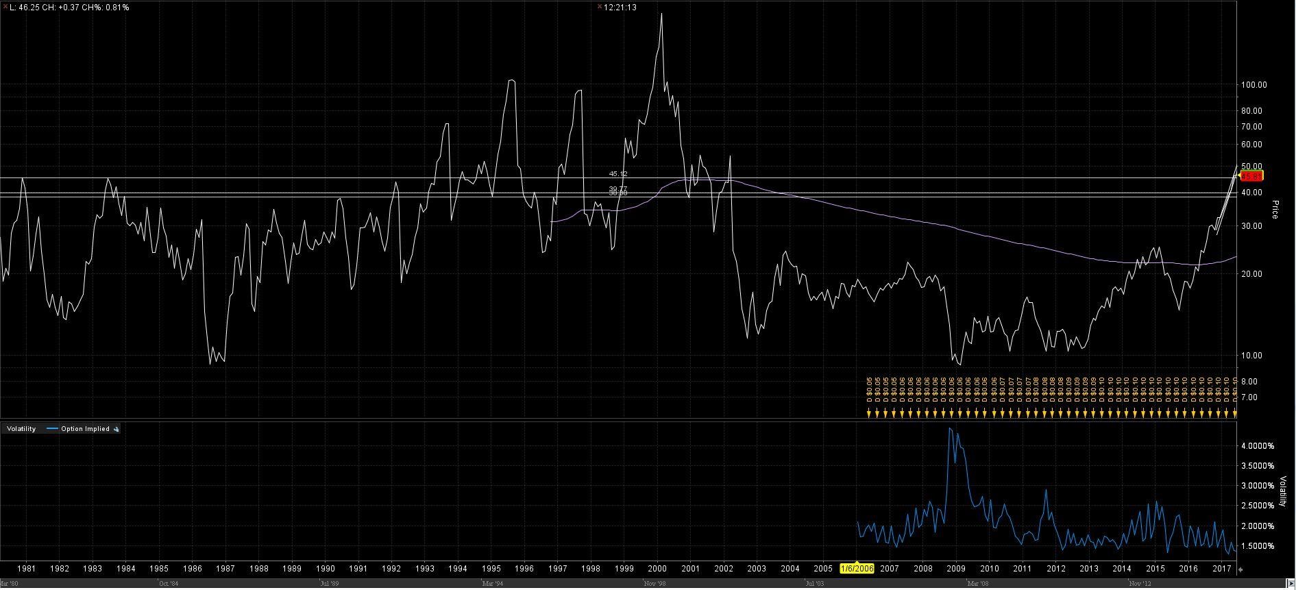
Bild passt nicht in den Beitrag

Antwort auf Beitrag Nr.: 52.501.474 von R-BgO am 30.05.16 12:12:30
war Ewigkeiten nicht mehr hier,
sollte vielleicht wieder öfter vorbeischauen
Antwort auf Beitrag Nr.: 59.013.844 von R-BgO am 21.10.18 13:11:39
deswegen Einstiegsposition
gekauft zu 29,97
Na das war ja was gestern :-) Zeitweise 10% im minus um dann im plus aus dem Handel zu gehen.
Applied Materials enttäuscht die Anleger
https://boerse.ard.de/aktien/applied-materials-enttauescht-d…
https://boerse.ard.de/aktien/applied-materials-enttauescht-d…
Antwort auf Beitrag Nr.: 59.019.835 von R-BgO am 22.10.18 13:43:54
-Acquisition provides Applied with complementary, leadership batch wafer processing systems business
-Increases Applied's global services business and strengthens customer support capabilities
-Immediately accretive to non-GAAP EPS upon closing
SANTA CLARA, Calif., July 01, 2019 (GLOBE NEWSWIRE) --
Applied Materials, Inc. ("Applied") (Nasdaq: AMAT) today announced a definitive agreement under which Applied will acquire all outstanding shares of Kokusai Electric Corporation ("Kokusai Electric") for $2.2 billion in cash from global investment firm KKR.
Kokusai Electric is a leading company in providing high-productivity batch processing systems and services for memory, foundry and logic customers. These systems complement Applied's leadership portfolio in single-wafer processing systems. Kokusai Electric has strong customer relationships, world-class supply chain and manufacturing capabilities in Japan and Asia, and a talented team of employees.
Following the close of the transaction, Kokusai Electric will operate as a business unit of Applied's Semiconductor Products Group and continue to be based in Tokyo, with technology and manufacturing centers in Toyama, Japan and Cheonan, Korea. The acquisition is expected to be immediately accretive to Applied's non-GAAP earnings per share at close.
The transaction has been approved by the Applied Materials Board of Directors. The transaction is expected to close within approximately 12 months and is subject to regulatory approvals and other customary closing conditions.
"Kokusai Electric has a strong culture of innovation along with excellent customer relationships and serves fast-growing areas of the wafer fab equipment market," said Gary Dickerson, president and CEO of Applied Materials. "By bringing Kokusai Electric's talented team into Applied, we believe we will accelerate innovation for customers and create significant value for our shareholders."
"The opportunity to combine with Applied Materials will be very attractive for Kokusai Electric's customers and employees alike," said Fumiyuki Kanai, president and CEO of Kokusai Electric. "We are excited about the opportunity to integrate Kokusai Electric's experienced team with Applied's global development, customer support and services capabilities. We believe the combination will accelerate our ability to bring exciting new technologies to customers."
Applied expects to finance the transaction using a combination of balance sheet cash and a term loan facility. Following the close of the transaction, the company will prioritize repayment of the term loan balance while maintaining its long-term commitment to return cash to shareholders through dividends and share repurchases.
Goldman Sachs & Co. LLC served as exclusive financial advisor, and Hogan Lovells and Cleary Gottlieb Steen & Hamilton LLP served as legal counsel for Applied Materials.
Applied Materials to Acquire Kokusai Electric
Date(s): July 1, 2019 6:00 AM-Acquisition provides Applied with complementary, leadership batch wafer processing systems business
-Increases Applied's global services business and strengthens customer support capabilities
-Immediately accretive to non-GAAP EPS upon closing
SANTA CLARA, Calif., July 01, 2019 (GLOBE NEWSWIRE) --
Applied Materials, Inc. ("Applied") (Nasdaq: AMAT) today announced a definitive agreement under which Applied will acquire all outstanding shares of Kokusai Electric Corporation ("Kokusai Electric") for $2.2 billion in cash from global investment firm KKR.
Kokusai Electric is a leading company in providing high-productivity batch processing systems and services for memory, foundry and logic customers. These systems complement Applied's leadership portfolio in single-wafer processing systems. Kokusai Electric has strong customer relationships, world-class supply chain and manufacturing capabilities in Japan and Asia, and a talented team of employees.
Following the close of the transaction, Kokusai Electric will operate as a business unit of Applied's Semiconductor Products Group and continue to be based in Tokyo, with technology and manufacturing centers in Toyama, Japan and Cheonan, Korea. The acquisition is expected to be immediately accretive to Applied's non-GAAP earnings per share at close.
The transaction has been approved by the Applied Materials Board of Directors. The transaction is expected to close within approximately 12 months and is subject to regulatory approvals and other customary closing conditions.
"Kokusai Electric has a strong culture of innovation along with excellent customer relationships and serves fast-growing areas of the wafer fab equipment market," said Gary Dickerson, president and CEO of Applied Materials. "By bringing Kokusai Electric's talented team into Applied, we believe we will accelerate innovation for customers and create significant value for our shareholders."
"The opportunity to combine with Applied Materials will be very attractive for Kokusai Electric's customers and employees alike," said Fumiyuki Kanai, president and CEO of Kokusai Electric. "We are excited about the opportunity to integrate Kokusai Electric's experienced team with Applied's global development, customer support and services capabilities. We believe the combination will accelerate our ability to bring exciting new technologies to customers."
Applied expects to finance the transaction using a combination of balance sheet cash and a term loan facility. Following the close of the transaction, the company will prioritize repayment of the term loan balance while maintaining its long-term commitment to return cash to shareholders through dividends and share repurchases.
Goldman Sachs & Co. LLC served as exclusive financial advisor, and Hogan Lovells and Cleary Gottlieb Steen & Hamilton LLP served as legal counsel for Applied Materials.
Beitrag zu dieser Diskussion schreiben
Zu dieser Diskussion können keine Beiträge mehr verfasst werden, da der letzte Beitrag vor mehr als zwei Jahren verfasst wurde und die Diskussion daraufhin archiviert wurde.
Bitte wenden Sie sich an feedback@wallstreet-online.de und erfragen Sie die Reaktivierung der Diskussion oder starten Sie eine neue Diskussion.
Investoren beobachten auch:
| Wertpapier | Perf. % |
|---|---|
| +0,87 | |
| +2,37 | |
| +3,43 | |
| -0,35 | |
| -0,50 | |
| +10,22 | |
| -9,20 | |
| +1,82 | |
| +6,18 | |
| +1,45 |
Meistdiskutiert
| Wertpapier | Beiträge | |
|---|---|---|
| 215 | ||
| 90 | ||
| 78 | ||
| 58 | ||
| 56 | ||
| 35 | ||
| 34 | ||
| 29 | ||
| 28 | ||
| 25 |


18.04.24 · dpa-AFX · Alaska Air Group |
18.04.24 · dpa-AFX · Applied Materials |
18.04.24 · dpa-AFX · Alaska Air Group |
18.04.24 · dpa-AFX · Applied Materials |
17.04.24 · dpa-AFX · Advanced Micro Devices |
17.04.24 · dpa-AFX · Advanced Micro Devices |
17.04.24 · dpa-AFX · Advanced Micro Devices |
21.03.24 · dpa-AFX · Applied Materials |
| Zeit | Titel |
|---|---|
| 11.03.24 |